The $0.50 question every hardware buyer faces

2-Layer PCB: are you paying for routing you don't need — or saving pennies on reliability you can't afford to skip?

Every month, procurement engineers send us Gerber files for a board that could have been built as a single-sided PCB with half a dozen wire jumpers. And every month we see designs that should have been four-layer boards but were squeezed into two layers to save $0.40 — only to fail EMC testing or need a respin.

The 2-layer (double-sided) PCB sits at an awkward middle: it costs roughly 40–60% more than a 1-layer board but 50–70% less than a 4-layer board of the same size. The question is not whether XFPCB can build it — we build thousands of double-sided designs every month. The question is whether a double-sided PCB is the right structural choice for your specific product, quantity, and risk tolerance.

This page exists to help you answer that question before you send a PO — not after you discover a problem on the assembly line.

FR-4 standard PTH vias 1 oz–2 oz copper HASL / ENIG / OSP Prototype to production
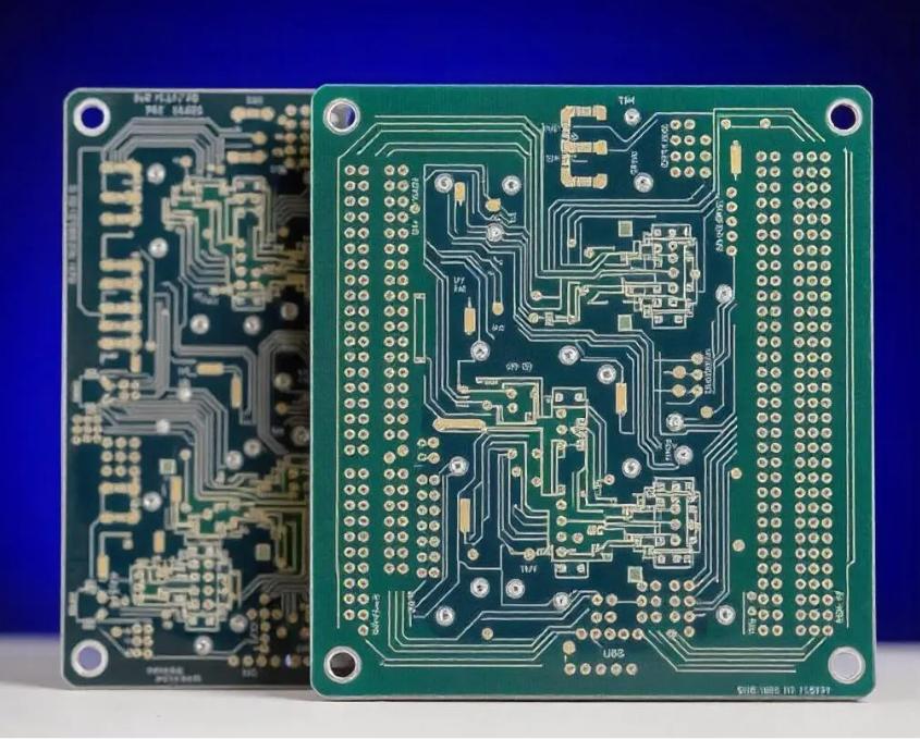
XFPCB 2-layer double-sided PCB fabrication
~40–60% cost premium vs 1-layer
50–70% less than 4-layer
2 copper layers
0.8–2.4 mm board thickness range
Decision framework

The three-way crossroads: which layer count fits your product?

Most layer-count decisions are made by inertia — "the last board was 2 layers" or "2 layers is cheapest." Here is a structured engineering framework to help you (and your team) choose with data instead of habit.

Stay at 1-Layer

Lowest $/board • Punchable at volume

Choose this when:

  • Trace count ≤ 15–20 with simple routing
  • Frequency < 10 MHz — no ground plane needed
  • Component count ≤ 30–40, all on one side
  • Volume > 10,000 pcs makes tooling worthwhile
  • Wire jumpers or zero-ohm resistors acceptable

Cross the wire-jumper threshold at ~8–12 jumpers/board; beyond that, 2-layer becomes cheaper.

Best fit: 2-Layer

Balanced cost • PTH routing • Both-side components

Choose this when:

  • Trace count 15–60, moderate routing complexity
  • Frequency < 50 MHz — ground plane on bottom possible
  • Components on one or both sides
  • Quantities from 100 to 50,000+ pcs
  • PTH vias replace wire jumpers for cross-side routing
  • You need assembly-ready boards without jumper labour

Most cost-effective when component density fits comfortably on two copper layers without excessive via fan-out.

Upgrade to 4-Layer

Higher $/board • Planes • Better EMI • Impedance control

Choose this when:

  • Signal frequency > 50 MHz or edges < 3 ns
  • Need controlled impedance (USB, Ethernet, RF, LVDS)
  • EMI/EMC pre-compliance is a concern
  • BGA or fine-pitch IC needs layer fan-out
  • Multiple power domains need dedicated planes
  • Board density exceeds comfortable 2-layer routing

The 4-layer jump adds 50–70% cost but can eliminate a respin that costs 10× the board price in engineering time.

Engineering insight: In our CAM reviews, roughly 30% of submitted 2-layer designs could be comfortably built as 1-layer boards with minor rerouting — saving 40–60% on board cost. Another 15% should really be 4-layer boards to avoid signal-integrity problems that appear during compliance testing. We flag both cases during DFM review so you can make an informed choice before production.
Cost vs. Performance analysis

When 2 layers win on cost — and when they lose on total project cost

Board price is only one number. The real calculation includes engineering time, assembly yield, compliance retests, and field failures. Here is how 2-layer and 4-layer compare across the dimensions that actually affect your project budget.

2-Layer PCB Cost index: 1.0× (baseline)
Board price (100 pcs, 100×80 mm)
~$0.80–1.20/pc
Routing complexity ceiling
Moderate — 40–60 traces comfortable
EMI / signal integrity
Adequate below 50 MHz with ground plane
Respin risk from SI issues Medium
Assembly yield (typical) 97–99%
Lead time (prototype) 3–7 working days
vs
4-Layer PCB Cost index: 1.5–1.7×
Board price (100 pcs, 100×80 mm)
~$1.20–2.00/pc
Routing complexity ceiling
High — 4 layers with internal planes
EMI / signal integrity
Good — internal GND/VCC reference planes
Respin risk from SI issues Low
Assembly yield (typical) 97–99%
Lead time (prototype) 5–10 working days

The total project cost equation

Board price × quantity + engineering hours × hourly rate + compliance retest cost × expected retests + field failure risk × liability cost.

A 2-layer board that saves $400 on 1,000 units but causes a 3-week EMC retest ($6,000–15,000 in engineering + lab time) has already cost more than upgrading to 4-layer boards for the entire run. XFPCB flags these risks during DFM review — we would rather help you choose the right structure upfront than build a board that fails your qualification.

100–500 pcs

Prototype / Validation

2-layer is often the right choice for functional prototypes where tooling cost is secondary to speed. Unless you already know 4-layer is required for SI or mechanical reasons.

500–10,000 pcs

Pilot / Low-volume production

The 2-layer sweet spot. At these quantities, the per-board savings vs 4-layer can fund additional testing or certification. Most IoT and industrial-control projects fall here.

10,000+ pcs

High-volume production

Cost pressure is highest here. If the board can be made on 1-layer with jumpers, that may be the right call. If it genuinely needs 2 layers, panelisation efficiency becomes the dominant cost lever.

DFM playbook

Five rules for designing a manufacturable 2-layer PCB

Double-sided boards present unique design challenges: no inner planes to distribute copper, PTH barrels as the only inter-layer connection, and both sides visible for soldering. These five rules address the most common issues we catch during CAM review.

01

Route without unnecessary vias

Every via adds cost, takes board area, and creates a potential reliability point. On a 2-layer board, many signals can route entirely on one side with careful component placement. Before adding a via, ask: can this trace reach its destination by swapping layers at a component pad instead?

DO Arrange components so that top-side traces stay on top and bottom-side traces stay on bottom. Use PTH component pads as natural layer-change points.
DON'T Drop random vias "just in case." Each unnecessary via adds $0.002–0.005 per hole and reduces routing channel availability on the opposite side.
02

Maintain copper balance across layers

Unlike 4-layer boards with solid internal planes, a 2-layer board has no "neutral" copper layer to absorb asymmetry. If one side has 80% copper fill and the other has 20%, the board will warp during reflow soldering, causing tombstoning and solder joint stress.

DO Aim for copper density within 20 percentage points between top and bottom. Use cross-hatch ground fills or thieving patterns to balance dense areas.
DON'T Leave one side almost empty while the other is densely routed. A 60:40 or 50:50 copper distribution target prevents warp.
03

Thermal relief on every PTH pad connected to a copper pour

When a PTH pad connects directly to a large copper pour (ground fill, power polygon), the heat from the soldering iron or wave flows into the copper plane instead of staying at the joint. This causes cold solder joints, especially on double-sided boards where the barrel must wet on both sides.

DO Use 4-spoke thermal relief spokes, each 0.3–0.5 mm wide, for any PTH pad ≥ 1.0 mm diameter that touches a copper pour.
DON'T Connect PTH pads to copper pours with a solid thermal connection unless the pad is a high-current terminal that needs maximum heat sinking.
04

Annular ring: the most overlooked dimension

The annular ring is the copper donut around a drilled hole on each layer. For 2-layer boards, the ring must survive drill registration tolerance on both top and bottom independently — there is no inner-layer redundancy. If the ring is too narrow, a drill breakout on either side turns the via into a side-connection that can crack during assembly.

DO Maintain minimum annular ring of 0.15 mm (6 mil) for standard production, 0.20 mm (8 mil) for higher reliability. Annular ring = (pad diameter − finished hole diameter) ÷ 2.
DON'T Use the minimum pad diameter your EDA tool allows. Many autorouters generate annular rings as small as 0.05 mm, which will likely break out during drilling.
05

Solder mask dams between fine-pitch pads

On a 2-layer board, both sides are available for SMT components. When two fine-pitch pads (pitch ≤ 0.8 mm) are close together, the solder mask web between them can be too narrow to stay in place during fabrication and soldering, leading to solder bridges.

DO Maintain minimum 0.1 mm (4 mil) solder mask web between pads. For pitch ≤ 0.65 mm, consider ENIG finish (flatter pads reduce solder bridge risk).
DON'T Use solder-mask-defined (SMD) pads for fine-pitch parts on a 2-layer board if you're using HASL finish — the uneven pad surface increases bridge risk.

XFPCB checks all five rules (and two dozen more) during CAM review. We send a DFM report before production, not after.

Send your files for DFM review
Specification explorer

Every spec choice: what it costs, what it buys you, when it matters

Rather than a static table, here is each manufacturing parameter explained by the trade-off it represents — so you can decide what to specify and what to leave at default.

Base material

Default: FR-4 (Tg 130–140°C)
FR-4 standard Baseline General-purpose electronics, appliances, IoT
High-Tg FR-4 (170°C+) +10–20% Lead-free assembly, multi-reflow, high-reliability
CEM-1 / CEM-3 −20–25% High-volume consumer, punchable, non-critical
Tip: For 2-layer boards, FR-4 is the safest default. High-Tg only matters if your assembly uses lead-free profiles >250°C or the board operates near 130°C.

Copper weight

Default: 1 oz (35 µm)
1 oz (35 µm) Baseline Standard signal and power up to ~2 A continuous
2 oz (70 µm) +30–40% Higher current (2–5 A), better thermal spreading
0.5 oz (18 µm) −5–10% Fine-line etching, dense routing, controlled impedance
Tip: 2 oz on both sides is possible but requires wider minimum trace/space (typically 0.2/0.2 mm vs 0.1/0.1 mm for 1 oz). Plan your trace geometry before specifying heavy copper.

Board thickness

Default: 1.6 mm (0.063")
0.8 mm +5–15% Thin devices, space-constrained enclosures
1.0–1.2 mm +0–5% Moderate thinness, some flexibility in connectors
1.6 mm Baseline Standard — best rigidity, best for PTH reliability
2.0–2.4 mm +10–25% Heavy components, high-current, extra rigidity
Tip: For 2-layer boards, 1.6 mm gives the best PTH barrel reliability because the aspect ratio (thickness ÷ drill diameter) stays manageable. Thin boards below 0.8 mm need smaller drills and tighter registration control.

Surface finish

Default: Lead-free HASL
Lead-free HASL Baseline Standard RoHS, good solderability, wave or reflow
ENIG +50–100% Fine-pitch SMT, flat pads, long shelf life, aluminum PCB
OSP −5–15% Flat pads, short storage (<6 months), pure SMT assembly
HASL (leaded) −5–10% Non-RoHS products, best wave solder wetting
Tip: For most 2-layer designs, lead-free HASL is the cost-effective sweet spot. Upgrade to ENIG only if you have fine-pitch ≤ 0.5 mm QFPs/BGAs or the board will be stored >6 months before assembly.

Minimum trace / space

Standard: 0.15/0.15 mm (6/6 mil)
0.15/0.15 mm (6/6 mil) Baseline Standard — 1 oz copper, good for most designs
0.1/0.1 mm (4/4 mil) +10–15% Denser routing, BGA fan-out, smaller boards
0.075/0.075 mm (3/3 mil) +20–30% Advanced density, premium fabrication
Tip: On a 2-layer board, you rarely need 3/3 mil unless you're routing very dense BGA fan-outs. Standard 6/6 mil handles most designs comfortably and gives better yield.

Hole size & PTH

Min mechanical: 0.3 mm
0.3 mm (12 mil) min drill Baseline Standard vias, small PTH components
0.25 mm (10 mil) min drill +5–10% Higher density, smaller vias
0.2 mm (8 mil) min drill +15–25% Premium density, advanced designs
Tip: Minimum hole size drives cost more than most buyers realise. A 0.3 mm drill bit lasts ~3× longer than a 0.2 mm bit before needing replacement. Use 0.3 mm as your default via size unless routing density forces smaller holes.
Physical structure

The anatomy of a 2-layer PCB

Understanding the cross-section helps you make better decisions about board thickness, copper weight, and dielectric spacing — especially when your design includes impedance-sensitive traces.

Top Solder Mask ~20–30 µm — LPI green (standard)
L1: Top Copper 1 oz (35 µm) — signal & components
FR-4 Core (Dielectric) 1.53 mm (1.6 mm total board minus 2 × 35 µm Cu)
L2: Bottom Copper 1 oz (35 µm) — signal, ground, & secondary components
Bottom Solder Mask ~20–30 µm — LPI green (standard)
PTH via drills through all layers, barrel-plated with copper to connect L1 to L2

Dielectric constant matters

FR-4 has a DK of ~4.5 at 1 MHz, dropping to ~4.2 at 1 GHz. For impedance-controlled traces on a 2-layer board, the dielectric thickness between L1 and L2 is fixed by the core — you cannot tune it independently as you can with prepreg in a multilayer stackup.

No internal planes

Unlike 4+ layer boards, a 2-layer PCB has no dedicated ground or power plane. The bottom copper must carry both signals and (optionally) a ground fill. This means return current paths are less controlled, which limits the board's signal-integrity ceiling to roughly 50 MHz for critical traces.

Copper balance

With no inner layers to absorb asymmetry, the copper distribution between L1 and L2 directly affects board flatness. A large copper imbalance (>30 percentage points difference) can cause visible bow and twist — especially on boards thinner than 1.0 mm.

Buyer applications

What real buyers build with 2-layer PCBs

Each application listed here represents actual RFQs XFPCB has fulfilled. The common thread: a double-sided board provides enough routing and component density while keeping the unit price within a commercial budget.

IoT sensors & gateways

Microcontroller + sensor + wireless module. 2-layer provides enough routing for the MCU, power regulation, and connector interfaces. Typical size: 30×50 mm to 60×80 mm.

Common finishes: HASL or ENIG

Industrial control interfaces

PLC I/O modules, relay drivers, signal conditioning boards. 2-layer handles the isolation gaps, high-current traces for relays/solenoids, and terminal block routing. Through-hole components common.

Common finishes: Lead-free HASL, 2 oz copper option

Power supply control circuits

AC-DC controller boards, DC-DC converter modules, motor drive interfaces. 2-layer copper can manage moderate heat and current. Thicker copper (2 oz) and wider traces for power paths.

Common finishes: HASL, 2 oz copper

Consumer electronics prototypes

Startup MVPs, validation prototypes, university research projects. Speed matters most. 2-layer PCB with standard specs, 3–5 day lead time, and progressive transition to production panelisation.

Common finishes: Lead-free HASL or OSP

Display interface boards

LCD/LED driver boards, touch controller interfaces, display adapter boards. 2-layer handles the parallel/serial traces and connector fan-out. Ground plane on bottom for noise reduction.

Common finishes: ENIG for fine-pitch FPC connectors

Sensor modules & breakouts

Temperature, humidity, pressure, gas sensor boards. 2-layer provides clear analogue signal routing separation, power filtering, and connector/pin-header layout. Small quantities common.

Common finishes: ENIG (corrosion resistance for sensors)
Quick answers

The six questions buyers ask most before ordering 2-layer PCBs

What's the real difference between 1-layer and 2-layer?

A 1-layer board has copper on one side only — cross-traces need wire jumpers or zero-ohm resistors. A 2-layer board has copper on both sides with plated through-holes (PTH) connecting them, so signals can cross without jumpers. This matters when your design has more than about 15–20 traces or components on both sides.

When should I upgrade from 2-layer to 4-layer?

When your signal frequency exceeds 50 MHz, when you need controlled impedance (USB, Ethernet, RF), when you have multiple power domains that need dedicated planes, or when your routing is so dense that you're fighting for space on both layers. If you're wondering whether you need 4 layers, send us your files — we can usually tell from the Gerbers.

Can XFPCB build 2-layer boards with controlled impedance?

Yes, but with limitations. On a 2-layer board, the dielectric between L1 and L2 is the full core thickness (~1.53 mm for 1.6 mm board), which makes 50 Ω traces quite wide (~1.4 mm on standard FR-4). For tighter impedance control or narrower traces, we recommend discussing your target before layout is finalised.

Do I need ENIG or is HASL fine?

For most 2-layer designs: lead-free HASL is fine. Use ENIG if you have fine-pitch components (≤0.5 mm pitch), if the board will be stored more than 6 months before assembly, or if you need perfectly flat pads for reliable SMT soldering. ENIG also provides better corrosion resistance for sensor and industrial applications.

What files do you need for a 2-layer PCB quote?

Gerber files (RS-274X format), NC drill files, a board outline layer, and a readme or email with your specification: board thickness, copper weight, surface finish, solder mask colour, quantity, and delivery country. If you have a stackup diagram or impedance requirements, include those too.

Can you quote both prototype and production quantities together?

Yes — and we recommend it. Sending both quantities in the same RFQ lets us review panelisation and cost structure across the whole product lifecycle, not just the first batch. We can quote a 100-piece prototype validation lot and a 5,000-piece production run on the same board design in one response.

Start your engineering review

Send your 2-layer PCB files for review & quotation

We review every incoming design for DFM issues, material fit, and cost optimisation — and send you a structured report before you commit to a PO. For 2-layer boards, the review typically takes 2–4 hours after file receipt.

1
Upload your files Gerber + NC Drill + specs
2
We review & respond DFM report + quotation within 4–24 hours
3
Approve & produce 3–7 day lead time after confirmation

What to include for a faster quotation:

  • Gerber files (RS-274X) and NC drill files
  • Board dimensions, thickness, copper weight, finish
  • Quantity (prototype + production if applicable)
  • Solder mask colour and silkscreen colour
  • Delivery country and preferred shipping method
  • Any impedance, material, or special testing requirements

We respect your IP. All design files are treated as confidential and deleted 90 days after project completion unless otherwise agreed.