Server / AI backplanes
Dense midplanes and backplanes that fan out many high-speed lanes plus heavy power planes. Layer count grows with SerDes count, reference plane pairing, and connector pin fields.

When routing density, power integrity, and high-speed channels no longer fit in a 24- or 32-layer stack, engineers move to 40-layer multilayer boards. XFPCB fabricates 40-layer PCBs for server and networking backplanes, dense BGA/HDI hybrids, and other high layer-count applications - with CAM review of stackup, copper balance, sequential press architecture, and drill/plating feasibility before production starts.
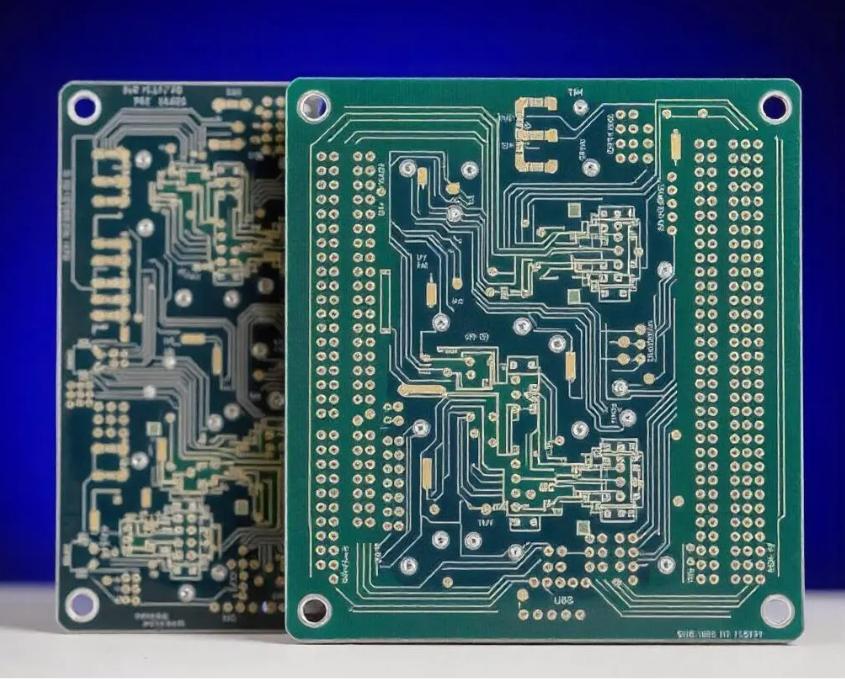
40 layers are chosen for interconnect density and channel count - not for marketing layer counts. Typical drivers are below.
Dense midplanes and backplanes that fan out many high-speed lanes plus heavy power planes. Layer count grows with SerDes count, reference plane pairing, and connector pin fields.
Switch and router line cards or chassis backplanes where differential pairs, power domains, and control planes must coexist without starving return paths.
High-reliability multilayers with strict material, registration, and documentation requirements. Builds are engineering-led with stackup and process review up front.
Fine-pitch BGAs that need buried vias, sequential build-up, and enough signal/power layers under the package footprint to escape without compromising SI/PI.
A 40-layer board is rarely a single-press FR-4 job. Thickness, registration stack-up error, resin fill, and high aspect-ratio plating all compound. Below is how we approach the main process risks - in practical manufacturing language, not speculative "physics marketing."
Most 40-layer designs need multiple press cycles (often 5 to 6+, depending on blind/buried via architecture). Sub-laminates are built, inspected, then combined so heat and pressure can cure each stage without extreme thermal gradients through a full 40-layer pack. Material selection must tolerate repeated thermal exposure above Tg without becoming brittle.
We review proposed press architecture early: which layers are cores vs. foil builds, where buried vias live, and how many sequential cycles the design truly needs. Extra cycles add cost and schedule; too few cycles can create voids, warp, or registration miss.
Each press cycle adds dimensional change from copper, glass, and resin CTE mismatch. Uneven copper density between layers (or between mirrored layer pairs) amplifies warp and local shift. For 40-layer work we:
Typical layer-to-layer registration targets for this class of board are on the order of +/- 2 to 3 mil (+/- 0.05 to 0.075 mm) for standard process control, with tighter targets available when the design and process plan support advanced compensation and verification. Exact limits depend on panel size, material set, and sequential architecture.
Finished 40-layer boards often land in the 4.0 mm to 7.0+ mm thickness range. That drives aspect ratio (board thickness / drill diameter). High aspect ratios need careful drill parameters, chip evacuation, and plating chemistry so barrel copper stays continuous at the mid-span - not only at the surface.
For high-speed channels we support depth-controlled back-drilling to shorten via stubs. Residual stub and depth tolerance are design- and stackup-dependent; we confirm achievable stub length during CAM review rather than promising a single universal number for every stack.
Common choices include high-Tg FR-4 for power/ground and mechanical strength, and low-loss laminates (for example Megtron-class, Tachyon, Astra MT77, or similar) on critical routing layers. Hybrid stackups are normal: put low-loss dielectrics where SerDes run, and cost-effective high-Tg cores where planes dominate. We do not claim exclusive proprietary chemistries - we qualify materials and press recipes that fit your impedance, loss, and reliability targets.
Honest working ranges for RFQ planning. Final limits are confirmed after stackup and Gerber review - panel size, copper weight, and via architecture all matter.
Even layer counts; sequential build-up as required by blind/buried vias
Thicker builds reviewed case by case with drill and plating feasibility
Tighter targets possible with advanced scale + X-ray process plan
Higher ratios evaluated with plating process and coupon microsection
Use these ranges for early design and RFQ. Align numbers with your stackup notes so CAM can confirm without surprise EQ cycles.
| Category | Parameter | Typical capability | Notes |
|---|---|---|---|
| Stackup | Layer count | 40 | Even counts; odd counts only with engineering review |
| Sequential press cycles | 5 - 6+ | Driven by buried via / HDI architecture | |
| Finished thickness | About 4.0 - 7.0 mm | Up to ~8.0 mm with extended tooling review | |
| Registration | Layer-to-layer (standard) | +/- 3 mil (+/- 0.075 mm) | Optical scale + process control |
| Layer-to-layer (advanced) | +/- 1.5 - 2 mil | Requires closed-loop scale and X-ray plan | |
| Panel size (max, process) | Up to about 610 x 457 mm | Usable area reduced by tooling strip / coupons | |
| Drill and plate | Min mechanical drill | 0.20 mm (8 mil) typical | 0.15 mm possible with aspect-ratio limit |
| Max PTH aspect ratio | 16:1 standard; ~20:1 advanced | Confirm with plating coupons on thick builds | |
| Back-drill depth control | +/- 2 - 3 mil typical | Stub length set by SI requirements | |
| Copper weight | 0.5 - 3 oz common; 4 oz reviewed | Heavy copper needs resin-fill planning | |
| Materials and finish | High-speed laminates | Megtron 6/7, Tachyon 100G, Astra MT77, similar | Hybrid stackups supported |
| High-Tg FR-4 | S1000-2, IT-180A, 370HR class | Tg typically 170 deg C+ | |
| Surface finishes | ENIG, Immersion Ag/Sn, OSP, LF HASL, hard gold | Select by assembly and shelf-life needs | |
| Quality | Electrical test | 100% netlist test | Flying probe or fixture as volume dictates |
| Cross-section / coupons | Available on request / as specified | Useful for plating and registration audits |
Process controls that matter most at this layer count - stated as manufacturer practice, not unverifiable lot claims.
Before tools are cut we review impedance targets, dielectric thicknesses, copper balance, resin fill risk, and sequential via architecture. The goal is to catch unbuildable or high-risk features while changes are still cheap.
Sub-laminate and final checks reduce the chance that registration or plating issues only appear at final test on an expensive panel.
Send a complete package and you get a faster, more accurate quote - and fewer engineering queries mid-build.
Layer order, copper weights, core/prepreg types, target thicknesses, and Dk/Df if impedance-controlled. Mark sequential press stages and buried via spans.
Complete RS-274X (or ODB++ / IPC-2581), Excellon drills with plated vs. non-plated clear, and IPC-D-356 or equivalent for electrical test.
Controlled-impedance tables, differential pair rules, back-drill layer maps, and any max stub length requirements for high-speed lanes.
Panelization preference, board outline and thickness tolerance, surface finish, solder mask/legend, IPC class, and any X-ray or coupon requirements.
Prototype vs. production qty, target date, and whether a first-article / engineering lot is acceptable before volume. High layer-count builds need realistic press cycle time.
Heavy copper islands, press-fit holes, edge plating, cavity, or hybrid RF materials - call these out explicitly so CAM does not miss them.
Plan on multiple weeks, not a few days. Sequential lamination, registration checks, and thick-board plating cannot be compressed arbitrarily without raising risk. After CAM receives a complete package we confirm a schedule for your specific stackup. Expedites are possible only when the press and verification plan still stay process-safe.
Yes - hybrid stackups are common. Low-loss laminates on SerDes layers and high-Tg FR-4 on power/ground can balance cost and performance. We review CTE compatibility, press temperature windows, and resin flow so the hybrid does not create warp or void risk.
Design annular rings and via-to-copper clearances assuming manufacturing registration on the order of a few mils layer-to-layer, then tighten only where the process plan (and cost) supports advanced compensation. Share critical BGA and buried-via alignment needs in the RFQ so we can map them to a realistic registration budget.
Yes. Provide a back-drill map (which drills, from which side, to which layer, and max residual stub). We confirm depth control capability against your finished thickness and SI requirements during engineering review.
Avoid unspecified "magic" tolerances, conflicting stackup notes, and drill sizes that ignore aspect ratio on a thick board. If a feature is critical, state the requirement clearly (registration, stub length, impedance, IPC class) and let CAM propose a buildable process rather than copying unverifiable competitor claims.
Send your stackup, Gerbers, and DFM notes. Our CAM team will review sequential lamination needs, registration and drill feasibility, and return a clear quote with engineering questions called out early.