
Choosing flying probe or a bed of nails is a method decision. It does not create access. Both methods, and a technician with a meter, only learn about copper they can land on. Design for test is the layout that makes that landing possible, and the written list of nets where you have accepted that it is not.
A pad the probe can hit
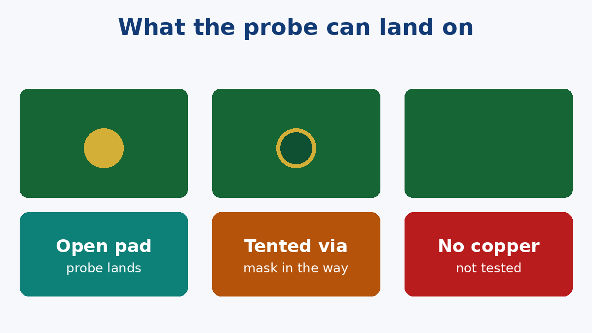
A test point is bare copper of a size and shape the chosen probe can sit on, with nothing tall beside it and no solder mask over it. A via is not automatically a test point. If the fabrication note tents the vias, the mask is what the probe hits, and the net reads open. If the same note says "use vias as test points," the two sentences contradict. Pick one: vias you will probe stay open, and the rest may be tented.
Which side the copper is on matters as much as the copper. A fixture with nails on one side never sees the other side. Points scattered on both sides mean a clamshell, a flip, or a method that can reach both sides. Ask that question before the layout freezes the pads onto the convenient side under a shield. A shield, a battery, or a connector body that covers the only pad has deleted the test, even if the pad is in the Gerber.
Flying probe and a bed of nails do not want the same pad. A nail is a spring pin in a fixture; it needs room from its neighbours and from tall parts, and the fixture vendor publishes that room. A flying probe is a moving needle and can often use a smaller feature, still with its own keep-out. Do not take a pad that was drawn for one and assume the other will accept it. Our Flying Probe Testing page is the fixture-free electrical check used on prototypes and low volumes. It still needs the copper exposed. It does not invent a pad you did not draw.
Which nets are worth a pad
"A test point on every net" is how dense boards lose their routing. The useful list is shorter, and it should be conscious:
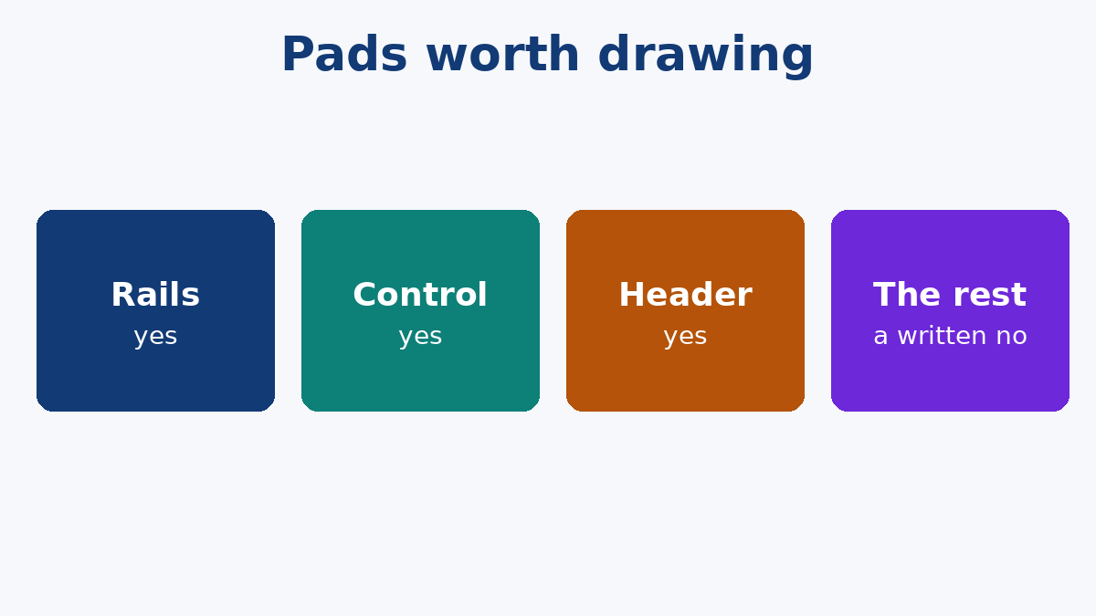
- Rails. Each power net, at a point that is actually that net and not on the far side of a ferrite or a 0-ohm you might remove. Ground in more than one place, so the fixture is not balancing the whole board on a single pad.
- The pins that let the board be quiet. Reset, enable, boot mode, and anything that must be held for the board to be in a known state while something else is measured.
- Programming and debug. The header you will use, with the pins named. A pad under the programming connector is not access if the connector is always fitted.
- Nets you will blame the assembly for. A sense line, a connector pin that has no other exposure, a net that has failed open before. If it has no pad, an open there is a debug project, not a test fail.
Everything else can be untested on purpose. Write that list down. An untested net discovered at shipment is a different event from an untested net you accepted at layout.
Nets that only exist as balls under a BGA are in the second category unless you fan a via out to a pad the probe can reach, or the pin sits on a boundary-scan chain. The ball is not a test point.
When the chain replaces the pad
IEEE 1149.1 boundary scan shifts data through a chain of digital devices and can see opens and shorts on pins that have no probe access. It is the right tool when the package hides the pins and you will not get a pad per pin. It is not a measurement of a capacitor, a resistor value, or a power rail. Those still want copper a probe can touch, or a functional check that powers the rail and watches what it does.
If boundary scan is the access plan, the factory and the test program need the chain itself: devices that are actually in the chain, the header, and the description file for each device. "JTAG it" on a board with no header and no chain is not a test method. It is a hope. Do not claim the electrical test covered the hidden pins unless that chain was built and run.
Put the access in the file, not in a sentence
Test pads are a solder-mask opening and, if they are probed after assembly, a spot the paste stencil does not flood. They belong in the Gerber, on a layer someone can find, with a note of which side is the probe side. A spreadsheet of net names that does not match the copper will be programmed as the spreadsheet, and the misses will look like board faults.
Our Manufacturing Files page is the package a build is quoted from, including Gerbers and the assembly notes. The test-point note belongs there: probe side, vias open or tented, nets deliberately without access, and whether the method is flying probe, a fixture, or a boundary-scan header. Leaving it out means the test coverage is whatever the program could reach, reported later as if it had been the plan.
Before the test method is chosen
- Exposed copper, one agreed size, clear of tall parts, on a side the method can reach.
- Vias are either probe points or tented, not both.
- Rails, grounds, control pins and the nets you care about have pads. Hidden balls do not count.
- Boundary scan is specified with a header and a chain, and it is not asked to measure passives.
- The untested list is written down, so a later open on that net is not a surprise.
The probe reports the copper it touched. Design for test is the decision about which copper that will be.