
The enclosure drawing landed before the schematic was finished. IP54 outdoor housing, limited airflow, and a connector wall that only opens on one face. The electrical team still talked about "a four-layer FR-4 board." The mechanical team talked about heat and water. The buyer asked for "whatever PCBs are used for this kind of product." That question is not a textbook definition. It is a construction choice: which board form and reliability class fit the environment the product must survive.
At a China fab, "what is this PCB used for" is the first filter on stackup, copper, finish, flex vs rigid, and which inspection notes belong on the traveler. A consumer wearable, an industrial drive, a medical monitor, and an EV power stage can all be "electronics," yet they demand different layer counts, different dielectrics, and different evidence that the board will hold up. This article is secondary original shop guidance for buyers and new product engineers who searched "what is a PCB used for" and need more than a definition: how end markets drive construction, and what to put in an RFQ once the use is clear.
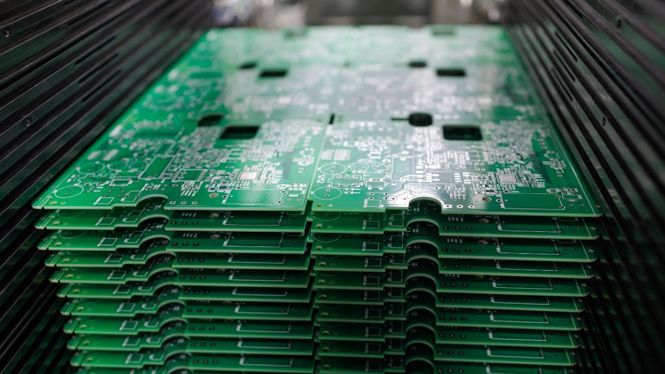
Shop anatomy: what a PCB actually is on the traveler
A printed circuit board is a laminated platform that holds components and routes power and signals through patterned copper. In shop language it is not "wires on plastic." It is a controlled stack of materials that must etch, drill, plate, mask, and assemble without yielding scrap.
The substrate (often FR-4 fiberglass/epoxy, sometimes polyimide flex film or a metal core) is the mechanical base and the insulator. Copper foil on one or more faces becomes traces and planes after imaging and etching. Vias -- plated holes -- stitch those copper layers so signals and power can move through the stack. Solder mask covers copper that should not take solder and reduces short risk. Silkscreen marks reference designators and polarity for assembly and field service. TechTarget-style layer models (substrate, copper, mask, silkscreen) map directly onto how CAM reads Gerbers: each layer file has a job on the line.
Components attach by through-hole (leads in plated holes, soldered) or surface-mount (pads on the same side). Most new volume designs lean SMT for density; THT still shows up on connectors, power parts, and harsh-environment boards where mechanical retention matters. High-density interconnect (HDI) adds microvias and finer features when phones, modules, or compact medical boards need more interconnect in less area. None of that anatomy is decorative. It is what the fab quotes against when you say consumer, industrial, medical, or EV.
What PCBs are used for -- by end market and fab stress
Printed circuit boards are used wherever electronics must connect components, distribute power, and keep signals honest inside a defined mechanical envelope. That spans consumer gadgets, vehicles, factory machines, medical instruments, telecom gear, energy systems, and aerospace electronics. The useful question for manufacturing is which stress dominates.
Consumer electronics and compact IoT push density, thin boards, and cost. Smartphones, wearables, tablets, and many appliances need short routes, fine pitch, and often HDI or rigid-flex so the board follows the housing. Fab stress is yield at fine line/space, warpage on thin cores, and assembly that stays clean at high pad density. Reliability class is usually commercial: important, but not the same documentation and life test depth as medical or automotive.
Industrial control and automation stress heat, vibration, and long duty cycles. Drives, PLCs, measurement gear, and machine controllers sit near motors, cabinets, and dirty air. Fab stress includes thicker copper or better thermal paths, higher Tg laminates when continuous temperature climbs, conformal coating notes when humidity or contaminants are expected, and mechanical retention for connectors. Buyers who only mark "FR-4, 4 layer" without vibration or temperature context get a commercial board that may pass first article and fail in the cabinet.
Automotive and EV add thermal cycling, vibration, and safety-adjacent reliability. Infotainment can look consumer-like; ADAS, ECUs, battery management, and traction inverters do not. Fab stress is material stability under temperature swing, copper that carries real current without hot necks, clear isolation where high voltage shares the outline, and process control that matches the customer's automotive quality expectations. Saying "EV" on an RFQ without naming BMS vs charger vs cabin module forces the fab to guess the wrong class.
Medical devices stress cleanliness, traceability, and controlled processes as much as electrical function. Imaging, patient monitoring, and diagnostic boards often need stable impedance, low contamination, and documentation that ties lot to process. Density can be high (including implant-adjacent or wearable form factors), but the fab cares about what you will audit: materials certs, cleanliness, and inspection depth -- not only layer count.
Telecom, 5G, and high-speed compute stress signal integrity and layer count. Routers, base stations, servers, and backplanes need controlled impedance, low-loss materials in RF or multi-gigabit paths, and enough layers for reference planes. Fab stress is stackup discipline, dielectric consistency, and drill/via structures that do not wreck high-speed returns.
Aerospace, defense, and energy systems stress environmental extremes and uptime. Vibration, shock, wide temperature, and remote serviceability show up in sensors, power supplies, navigation, grid controllers, and storage electronics. Construction may lean rigid-flex for packaging, high-Tg or specialty materials for heat, and inspection/test notes that match the reliability claim. Synopsys-style industry spans (hi-tech/5G, aero/defense, automotive/EV, energy, industrial harsh environments) are useful labels only when you translate them into those fab stresses on the quote form.
Layer count and form factor as answers to stress
Layer count and board form are how engineering answers the stresses above -- not vanity metrics.
Single-sided and double-sided boards still serve simple appliances, LED drivers, and low-density controls when routing is light and cost dominates. Multilayer boards (4, 6, 8+) add planes for power integrity, EMI control, and routing escape under fine-pitch parts. HDI and higher layer counts appear when the product outline shrinks faster than the netlist.
Rigid FR-4 (or high-Tg FR-4) is the default when the housing is fixed and heat is manageable with copper and airflow. Flexible circuits earn their place when the board must fold into a hinge, wrap a battery, or survive repeated flex -- common in cameras, wearables, and some medical and vehicle modules. Rigid-flex combines stable component areas with flexible interconnect so connectors and cables drop out of the BOM. Metal-core (MCPCB) boards answer concentrated heat in LED engines and compact power stages when the metal base can couple to a sink or chassis. Ceramic constructions sit further out when temperature or reliability leaves organic laminates behind.
Match form to the product decision that started this article: enclosure volume, bend or cable elimination, heat path to the case, and whether vibration will work connectors loose. A four-layer rigid board in a sealed hot box is a different job from a rigid-flex stack that frees the same schematic from three board-to-board cables.
Fab steps that matter for yield and scale
Full process tutorials belong elsewhere. For application-driven buys, only a few fab steps explain why "same circuit, different use" quotes differently.
Imaging and etching set whether fine consumer densities or thicker industrial copper can hold yield. Layer lamination under heat and pressure decides whether a high-layer or rigid-flex stack stays flat and registered. Drilling and plating create the vias that carry current and heat; aspect ratio and plating quality show up later as intermittents under vibration or thermal cycle. Solder mask and surface finish prepare the board for SMT or mixed assembly and for the environment (humidity, handling, shelf life) the use case implies. When volume scales, panelization, balanced copper, and repeatable stackups matter as much as the first prototype that "worked on the bench."
Those steps are why a China fab asks about use early. Consumer density fights etch yield. EV current fights copper weight and via plating. Medical and industrial reliability fight process variation that a hobby board never measures.
What to put in the RFQ once the use is clear
When you know the product environment, write the RFQ so CAM does not reverse-engineer intent from a lonely layer count.
State the end use in one plain line: consumer handheld, industrial cabinet IP54, medical patient vicinity, EV BMS, outdoor energy controller, and so on. Name the dominant stresses: temperature range, vibration/shock, humidity or contaminants, continuous vs intermittent power, and any safety or quality system the product must meet. Call the construction you believe fits -- rigid layer count, flex or rigid-flex, MCPCB -- and invite DFM pushback if the outline or heat path disagrees. List copper weights, min trace/space, impedance or HV isolation only where they apply, surface finish, and inspection/test expectations tied to that use (AOI only vs flying probe, X-ray on BGA, lot traceability). Attach Gerbers, stackup table, and notes that admit enclosure and environment drove the board type.
XFPCB quotes from that package in a factory-to-buyer voice: applications and industry context first, then a buildable stack. A clear use statement is not marketing copy. It is how layer count, flex, and reliability class get chosen before copper is etched.