
CAM rarely rejects a board for using the words "controlled impedance." What stops the quote is a fab note that stops at those two words. The package arrives with Gerbers, a layer count, and a sentence that says impedance is required--but no target ohms, no tolerance, no layer/reference map, and no rule for who may change width. CAM parks the job until engineering and purchasing close the gap.
That hold is not pedantry. Impedance is a stackup-plus-geometry agreement. USB, PCIe, DDR, Ethernet, and RF feeds all behave like transmission lines once edge rate and length make reflections matter. A short low-MHz net on a dense board may not need formal control; a compact SerDes route often does. The buyer test is simple: if the fab can change line width by a few mils or swap dielectric thickness to a "standard" stack without asking, does signal margin, timing, antenna tuning, or customer qualification move? If yes, the note on the drawing is incomplete.
This article stays on the shop-floor side of that gap: what a complete impedance table looks like on a real fab drawing, who owns geometry changes, how coupons and TDR prove a lot in buyer language, and which etch, mask, and glass-weave traps show up as failed TDR long after the quote looked clean.

What CAM asks when the note is incomplete
On a China fab floor, the first impedance EQ is almost always a list, not a lecture:
- Target impedance and structure (50 ohm single-ended, 90/100 ohm differential, CPW, etc.)
- Numerical tolerance (standard +/-10%, or a tighter call that must be paid for in process)
- Signal layer and reference plane(s) for each controlled structure
- Net group or structure ID CAM can match to copper
- Stackup locked or supplier-proposed--and which materials are substitutable
- Solder-mask modeling assumption for outer microstrip
- Geometry authority: preserve layout, or propose width/spacing changes before CAM release
- Coupon and TDR report expectation for the lot
Missing any of those fields does not mean every supplier will refuse. It means each supplier will invent a different assumption and still quote the same phrase. That is how two "controlled impedance" quotes compare apples to oranges--and how silent width changes land in production without engineering seeing them.
What a complete impedance table looks like on the fab drawing
Treat the impedance table as a manufacturing contract line, not a reminder. Each row should answer what CAM will etch, what stackup it rides on, and what evidence ships with the lot.
| Field | Example line | Why CAM needs it |
|---|---|---|
| Target | 100 ohm differential | Electrical goal, not a slogan |
| Tolerance | +/-10% (or customer value) | Sets process window and report accept band |
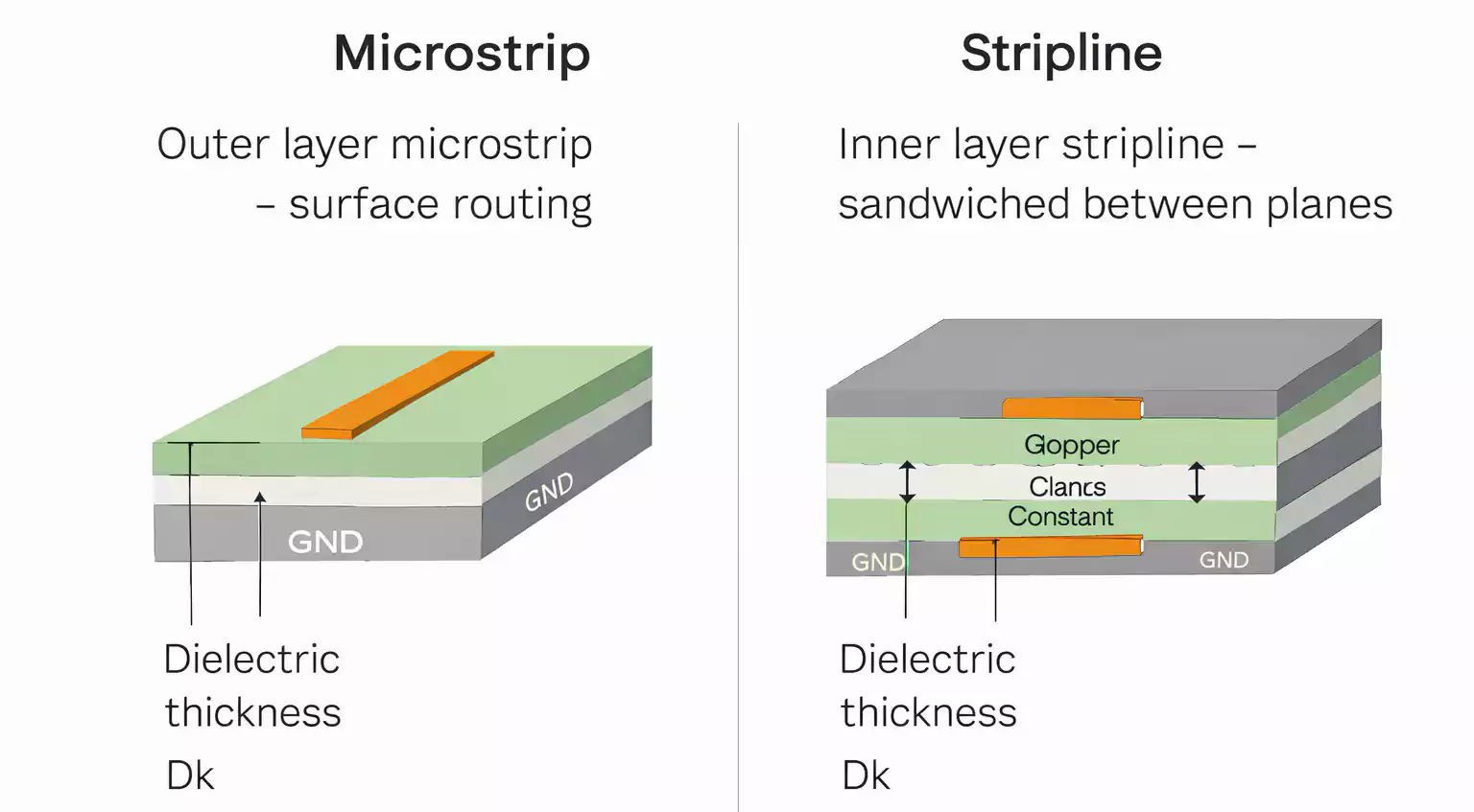
| Layer / geometry | L3 edge-coupled stripline | Ties ohms to dielectric and copper |
| Reference | L2 and L4 planes continuous | Prevents wrong return-path model |
| Nets / structure | USB3_TX/RX pair group | Matches copper CAM may not rename |
| Mask model | Outer microstrip: mask ON in calculation | Stops 2-5 ohm outer-layer surprises |
| Geometry authority | Supplier may propose width/spacing; engineering must approve before CAM release | Blocks silent artwork edits |
| Coupon / report | TDR per lot; coupon mirrors stackup; outer after soldermask | Defines lot evidence, not a post-ship favor |
A usable fab note sounds like: L1 microstrip 50 ohm +/-10% single-ended, mask included in model, referenced to L2; L3 stripline 100 ohm +/-10% differential, referenced to L2/L4; layout widths are starting values; supplier may return proposed width/spacing with calculated Z for approval; coupons required; TDR report with each lot.
If the drawing only says "controlled impedance required," expect a hold. If prototype and production differ (waived report, supplier stackup, temporary geometry), write the exception and close it before volume--prototype shortcuts that stay invisible become production assumptions.
Stackup first, then geometry authority
Impedance is not a trace-width checkbox you paste after routing. Lock the stackup before the critical pairs fan out: layer count, signal locations, copper weight, dielectric thickness, and named material family (FR-4 grade, high-Tg, low-loss, Rogers-class, etc.). Field-solver widths only mean something against that stack. Outer microstrip and buried stripline rarely share the same mil width for the same ohm target--and differential spacing is part of the electrical model, not decoration.
Then decide who may change geometry. Two authority models are common:
- Target-first: designer states ohms and tolerance; fab may adjust width/spacing inside manufacturable limits and returns the proposed numbers for engineering approval before CAM release.
- Preserve-layout: designer freezes artwork; fab reports whether the target is manufacturable on the locked stack and does not edit copper without a written ECO.
Either model works. The failure mode is the silent middle: one quote preserves your 5.1 mil pair, another quietly opens to 5.6 mil to hit 100 ohm on their prepreg, and purchasing thinks both "met impedance." Put the approval sentence on the drawing: supplier may adjust controlled traces only after returning proposed width, spacing, dielectric, copper, and calculated impedance for engineering sign-off.
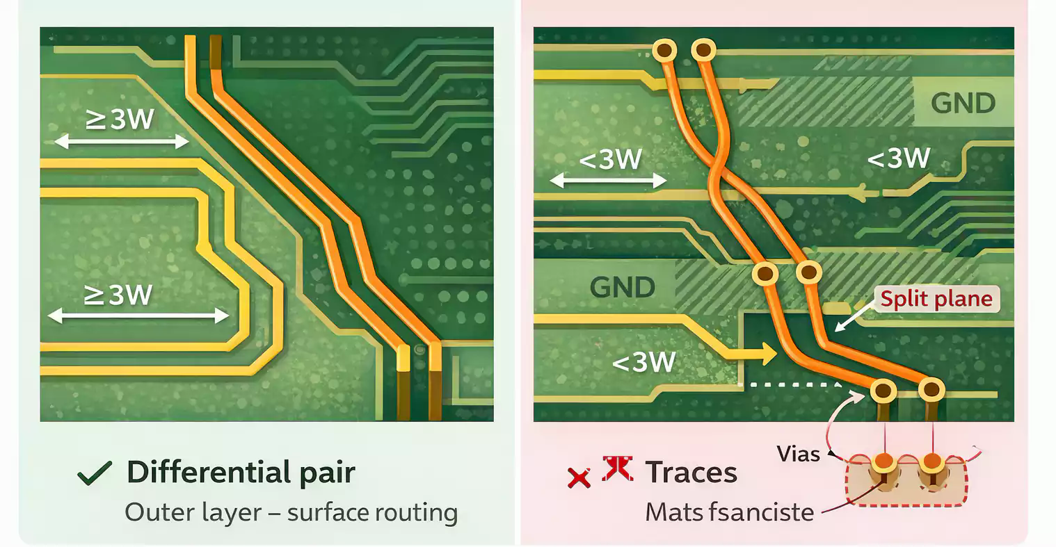
Routing still has to give CAM a clean return path. Keep differential pairs symmetrical, respect roughly 3W clearance from aggressors (tighter for sensitive pairs), do not cross split planes, and minimize via transitions. Coupons and TDR will not rescue a layout that routes over gaps or breaks pair symmetry at every BGA escape.
How coupons and TDR prove the lot (buyer language)
Buyers should ask what the report proves--and what it does not. Coupons are dedicated structures on the same panel as the production boards. They mirror the controlled stackup and geometry. TDR (time-domain reflectometry) launches a fast step into the coupon and reads impedance versus distance. Industry practice follows coupon architectures in the IPC-2141A family and measurement method language such as IPC-TM-650 2.5.5.7. Product nets are not probed; cutting into customer copper is not lot verification.
What a usable lot package includes:
- Coupon that matches the production stackup layer-by-layer (same construction, not a generic lab coupon)
- Enough length for a readable flat zone--about 150 mm minimum is a practical shop floor rule of thumb; longer is better when panel space allows
- Placement that respects panel variation (center vs edge dielectric and etch can differ); critical jobs often want more than one coupon location
- Outer-layer microstrip tested after soldermask when production boards ship masked
- Report tied to job/revision, layer, structure, target, tolerance, measured flat-zone value, and accept/reject--not a naked screenshot
TDR proves the lot's stackup and process landed inside the agreed band for the coupon structure. It does not prove every via stub, every length-match serpentine, or every connector launch on the product is perfect. Cross-section of first article still matters when geometry, etch factor, or dielectric height is disputed: field-solver prediction, measured cross-section, and TDR should tell a consistent story within a few ohms. If they disagree systematically, the model--not the operator--is usually wrong (mask omitted, wrong Dk, etch undercut ignored).
Etch, mask, and weave traps that fail TDR
When TDR comes back out of band, CAM and process usually look here first--not at abstract SI theory.
Etch factor. Wet etch undercuts resist. Artwork that says 4.0 mil can land nearer 3.0 mil after etch-back, raising impedance by roughly a tenth of the target on thin lines. Fabricators compensate artwork; coupons exist to prove the compensation matched the lot. A TDR trace that trends upward along the coupon often points to narrowing copper.
Soldermask loading. Outer microstrip sees a few ohms of capacitive loading from mask. If the coupon is measured bare while production ships masked--or if the designer modeled mask-off while CAM modeled mask-on--outer layers fail for paperwork reasons, not mysterious SI. Spec "test after soldermask" for outer controlled structures.
Glass weave. FR-4 is glass bundles in resin, not a uniform dielectric. Traces over glass vs resin-rich gaps see different effective Dk; periodic ripples on TDR often match weave pitch. Critical layers may need spread-glass or weave-aware routing; pretending FR-4 is homogeneous is how +/-3-5% "mystery" variation shows up inside a single panel.
Panel placement. Prepreg flow, etch chemistry, and plating distribution vary center-to-edge. One coupon in a lucky corner can pass while the product region sits elsewhere. Ask where coupons sit relative to your critical boards when the program is tolerance-sensitive.
Tolerance cost reality. +/-10% is the everyday fab window. +/-5% is a process program: tighter dielectric control, LDI-level imaging discipline, often better glass, and statistical control--not a free checkbox. Calling +/-5% without budget or stackup authority is a common quote breaker.
Controlled dielectric vs controlled impedance. Controlled dielectric means you lock thicknesses and materials. Controlled impedance means the fab tunes geometry (within your authority model) and proves the lot with coupons/TDR. Confusing the two is how buyers order "exact stack" and expect ohms without giving geometry authority--or order ohms and forbid any width change while freezing an unmanufacturable stack.
Close the quote before copper hits the press
A controlled-impedance RFQ that wins trust looks boring on purpose: impedance table with every field filled, stackup drawing attached, mask assumption stated, geometry approval path written, coupon/TDR scope priced in, and prototype exceptions listed so they cannot sneak into production. What gets rejected or held is the two-word note, conflicting notes across files, missing tolerance, silent geometry edits, outer coupons tested bare, and +/-5% language with no process budget.
XFPCB reviews impedance jobs the same way CAM does on the floor--table completeness, stackup lock, authority to adjust, and lot evidence--not as a marketing label on a quote. Send Gerbers, stackup, impedance table, and whether width may change under written approval so the quote matches the board you intend to ship.