
The SMT line opens a copper-base LED lot and the traveler already has a complaint sticker: after first reflow the copper base looks reddish, dull, or blotchy. Buyers ask whether the metal core is scrap. On the floor the first question is not "did the laminate fail"--it is whether the exposed copper oxidized because the Organic Solderability Preservative (OSP) never protected it, or because the film was thin, contaminated, or overheated.
Copper-base and other metal-core PCBs (MCPCB) put large copper areas in view for heat spreading. Those surfaces oxidize fast in a reflow furnace when bare. Mild color shift is often cosmetic. Heavy oxide is a solderability and thermal-pad risk. This article walks that call the way a factory does: oxidation versus scrap, what OSP actually does on copper pads, LED heat-path voids when OSP fails, storage and open-bag rules buyers must enforce, and when to leave OSP for ENIG.
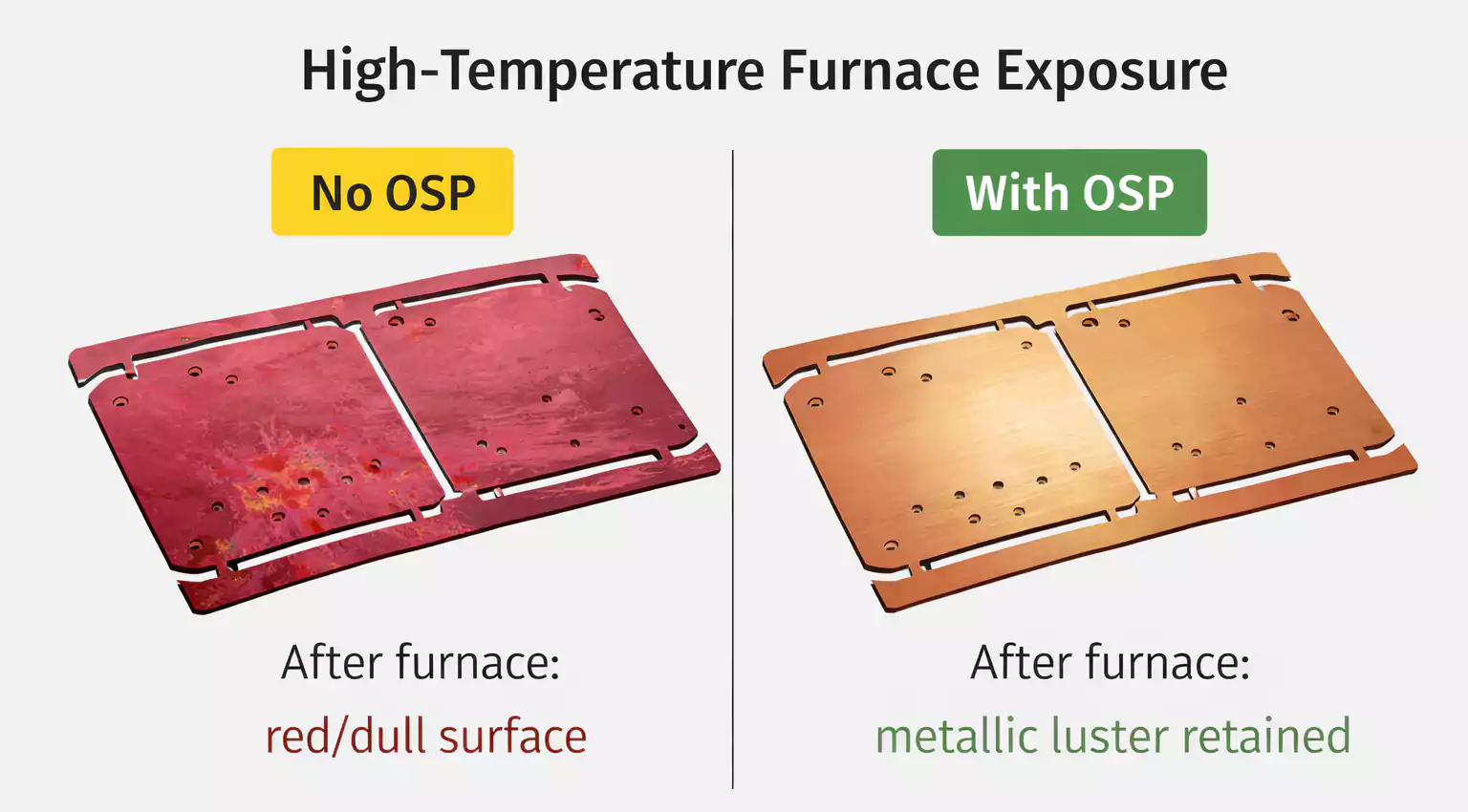
Red after reflow: oxidation call, not automatic scrap
Copper reacts with oxygen and moisture. Room-temperature film grows slowly; furnace heat accelerates Cu2O / CuO formation. Copper-base LED boards amplify the visual effect because:
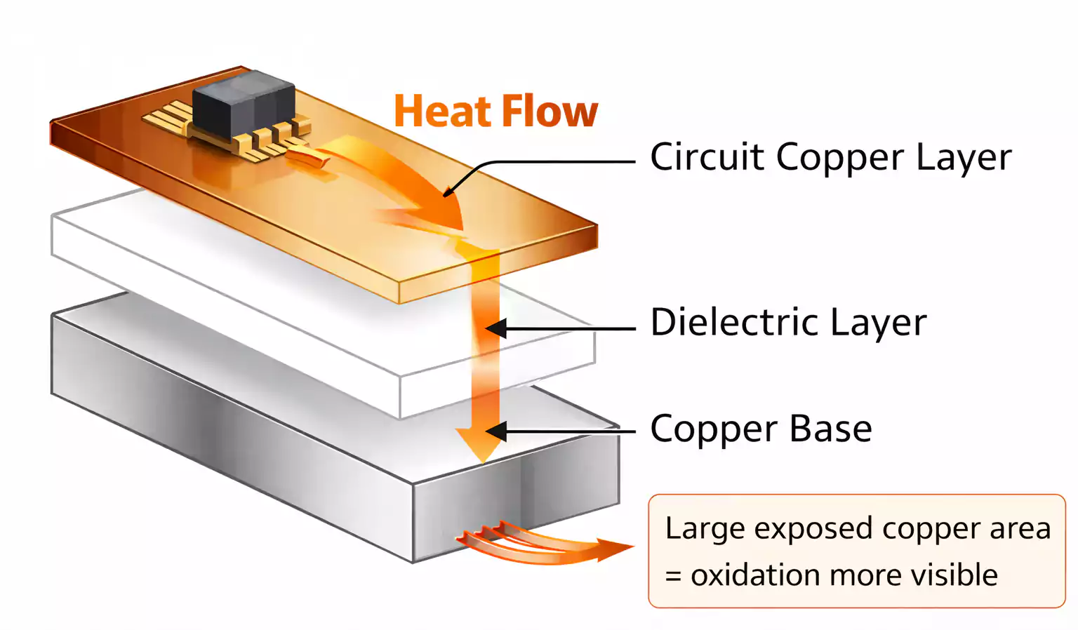
- Large thermal copper is left exposed for conduction, not buried under solder mask
- Furnace air (or weak nitrogen) hits that copper for the full profile
- Finger oils, etch residue, or uneven micro-etch make local patches darken first
Mild discoloration -- pale amber to light brown with still-bright pad texture -- is often a thin oxide. Flux can still wet; joints may pass AOI and functional test. Treat it as a process signal: review OSP age, bag integrity, glove discipline, and peak/time above liquidus.
Severe oxidation -- dull brown to black, patchy, fingerprint ghosts, or pads that refuse paste wetting -- is a scrap-or-recondition decision. Dewetting, solder beading, and thermal-pad voids follow. Do not "bake it clean." Baking OSP destroys the remaining organic film and makes the next reflow worse.
Factory triage on an incoming complaint:
- Compare sealed-bag photo vs post-reflow photo of the same panel ID
- Check date code, vacuum seal, HIC, and whether the bag sat open on the SMT rack
- Spot-check pad color under magnification: bright amber vs dull brown/black
- Run a coupon or scrap board through paste + profile before releasing the lot
- If wetting fails, strip/recoat OSP at fab or remake--do not invent a bake cure
Discoloration alone is not proof the dielectric or copper thickness is wrong. It is proof the surface chemistry left the copper unprotected when heat arrived.
What OSP does on the shop floor
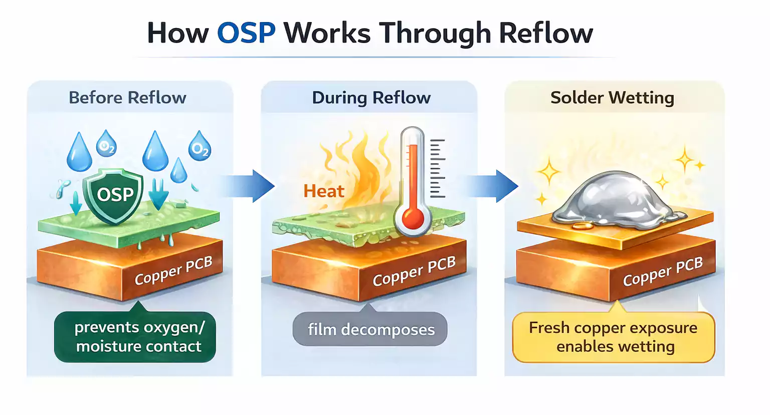
OSP is a thin azole-based organic film (typical target about 0.2-0.5 um) bonded to clean copper. It is not a metal plate. The shop sequence is:
- Clean / degrease -- remove oils and light oxide
- Micro-etch -- remove roughly a micron-scale copper skin so the film can grip
- Coat -- immerse or spray OSP chemistry; film grows until copper is sealed
- Rinse and dry -- set a transparent, copper-toned pad finish
During reflow, solder-paste flux dissolves that film so molten alloy meets fresh copper and forms Cu-Sn IMC. Flatness stays excellent because almost no metal thickness is added--useful for fine-pitch LED packages and dense SMT on the circuit side of a metal-core stack.
Compared with HASL or ENIG on the same copper-base job:
| Finish | Flatness | Typical sealed shelf life | Cost / process | Fit on copper-base LED |
|---|---|---|---|---|
| OSP | Excellent (near bare Cu) | About 3-6 months sealed | Low | High-volume, short warehouse dwell, planned SMT |
| LF-HASL | Uneven domes | 12+ months | Low-moderate | Longer storage; weak for fine pitch |
| ENIG | Excellent | 12+ months | Higher | Long storage, outdoor/harsh logistics, multi-reflow, gold-finger needs |
OSP still fails on copper base when clean/micro-etch is weak, film thickness is uneven, boards are handled bare-handed, thermal exposure is extreme, or contamination lands after coat. Multiple reflows and aggressive bake cycles chew through un-soldered film. Gold fingers, wear contacts, and castellated modules are the wrong place for OSP--specify ENIG or hard gold there instead.
LED heat-path risk when OSP fails
On copper-base and aluminum MCPCB LED boards the solder joint is part of the thermal path:
LED junction -> solder joint -> copper pad -> dielectric -> copper or aluminum base -> heatsink
Oxidized pads wet poorly. Paste balls up, leaves voids under thermal pads, or forms cold / incomplete joints. Voids block heat; junction temperature rises; lumen drop, color shift, and early LED death follow--even when the electrical net still "lights up" at ICT.
Buyers should treat OSP quality as a thermal reliability control, not a cosmetic preference:
- Match pack size to one SMT batch so leftover panels are not left open overnight
- Prefer nitrogen or proven flux activity when the design needs a second reflow soon after the first
- X-ray or void criteria on high-power LED thermal pads when the application is lumen-critical
- Reject lots with dull brown pads before paste print rather than arguing after AOI fails
ICT probes can also struggle on un-fluxed OSP testpoints because the film is insulating until flux or aggressive probes break through. Plan testpad finish or probe strategy accordingly.
Storage, open-bag, and no-bake rules buyers must enforce
OSP logistics fail more projects than OSP chemistry. Put these rules on the PO and the SMT work instruction:
Sealed life -- Plan on roughly 3-6 months solderable life in intact moisture-barrier bags with desiccant and HIC, stored cool and dry (keep warehouses under about 30 C / 60% RH; tighter climate control is better). Do not treat OSP like ENIG "ship and forget for a year."
Open-bag clock -- After the seal breaks, target first reflow inside 24 hours; treat 48 hours as a hard practical limit unless boards go straight into a dry cabinet or are resealed correctly. Double-sided builds: finish the second pass within about a day of the first while remaining pads are still workable.
No bake OSP -- Do not bake OSP boards to "dry them out." Oven heat degrades the organic film and leaves copper naked. Moisture control is packaging and FIFO, not a bake recipe copied from HASL docs.
Handling -- ESD gloves only. Finger salts and oils punch holes in a sub-micron film and print as dewetted fingerprints after reflow.
FIFO and pack size -- Align fab ship date to SMT week. Ask for bag quantities that match one line run so opened leftovers are not the default inventory mode.
Incoming inspection -- Good OSP pads look bright, uniform, pale amber / copper. Dull brown-black or smudged pads need solderability check (J-STD-003 style or a live reflow coupon) before the lot enters paste print. Expired or failed boards may be reconditioned by stripping OSP, micro-etching, and recoating--only if copper is not deeply corroded. Otherwise remake.
When to abandon OSP for ENIG on copper-base work
Keep OSP when assembly is scheduled soon after fab, cost and flatness matter, storage is controlled, and the design does not need many thermal cycles or edge contacts.
Move to ENIG (or another durable finish) when any of these are true:
- Boards will sit weeks to months in overseas transit plus warehouse before SMT
- Outdoor, marine, or uncontrolled humidity logistics are normal
- The product needs more than a couple of reflows / rework passes on the same pads
- Gold fingers, sliding contacts, or late hand-solder of castellations are on the board
- Your SMT site cannot enforce glove, dry-pack, and 24-48 h open-bag discipline
- Prior lots already show thermal-pad voiding tied to oxidized OSP pads
OSP remains a solid default for many copper-base LED and power modules when the factory and the buyer share one production calendar. It is a poor default when the calendar is fiction.
Further reading
- Aluminum PCB Guide: Thermal Design, Stackup Choices, and LED DFM
- Cold Solder Joints on PCB Assemblies: Causes, Inspection, Rework, and Prevention for Buyers
- BGA Soldering for Overseas Buyers: Reflow Profiles, X-Ray, and Void Limits
- PCB Conformal Coating for Buyers: Material Choice, Masking, and Process Control