
The first quote back from the fab is usually where the story breaks. A consumer-electronics team ports an aerospace-looking rigid-flex stack into the RFQ: thick polyimide, heavy hole-wall copper, bookbinder-style bend notes, generous layer count, and a reliability checklist written for flight hardware. CAM returns NRE for special materials, extra plasma/desmear steps, long lamination cycles, and a yield assumption that makes the unit price look nothing like a phone, earbud, or display-module budget.
That sticker shock is not the fab being difficult. It is the fab telling you consumer rigid-flex is a different product class. The goal is same-net packaging efficiency at volume--dense routing, thin construction, controlled cost--not maximum reliability at any cost. This article starts from that RFQ mismatch, then walks what consumer rigid-flex actually needs, which density-cost levers show up on real quotes, and which process windows protect yield before you lock Gerbers.
Why the aerospace copy fails a consumer RFQ
Aerospace and other high-reliability rigid-flex programs often favor thicker films, heavier plating, wider process margins, and constructions that protect bend life over decades. Consumer products ask for the opposite balance:
- thinner envelopes and folded 3D packaging
- denser SMT in rigid islands
- fewer connectors and discrete FPCs
- panel efficiency that survives tens or hundreds of thousands of units
- reliability that matches product life and warranty--not overbuilt margin that kills yield
When you paste aero language onto a CE drawing package, fab engineers still have to quote the literal stack. Expect sticker shock on material callouts above consumer norms, irregular outlines that destroy panelization, and bend constructions that need dedicated tooling. The RFQ fix is to rewrite the target: density + thinness + volume cost, with reliability stated as a use-case window (static fold vs dynamic hinge, temperature, drop, humidity).
What consumer electronics rigid-flex actually needs
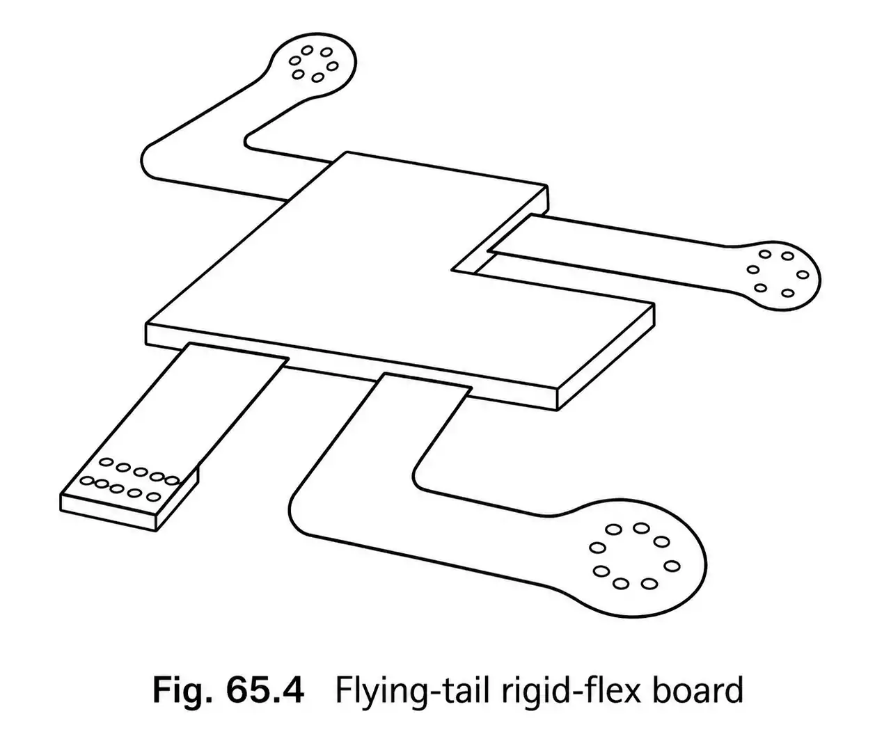
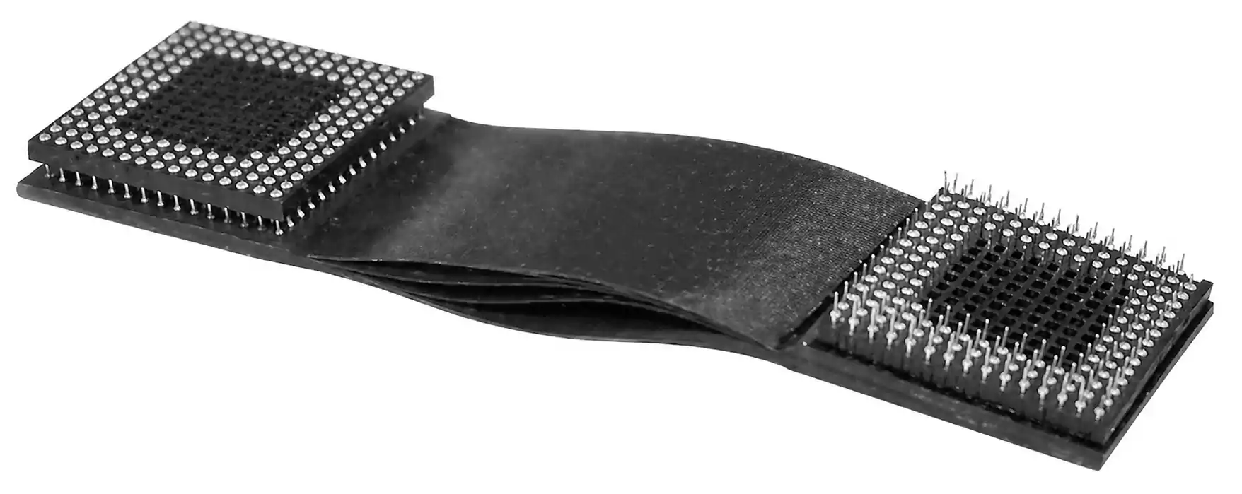
A practical CE rigid-flex is an interconnect system, not a bendable FR-4 substitute. Rigid sections carry dense SMT, small packages, and mechanical support. Flex sections provide fold, turn, and module-to-module routing so you can drop connectors and cable assemblies.
Typical shop-floor traits we see on volume-oriented builds:
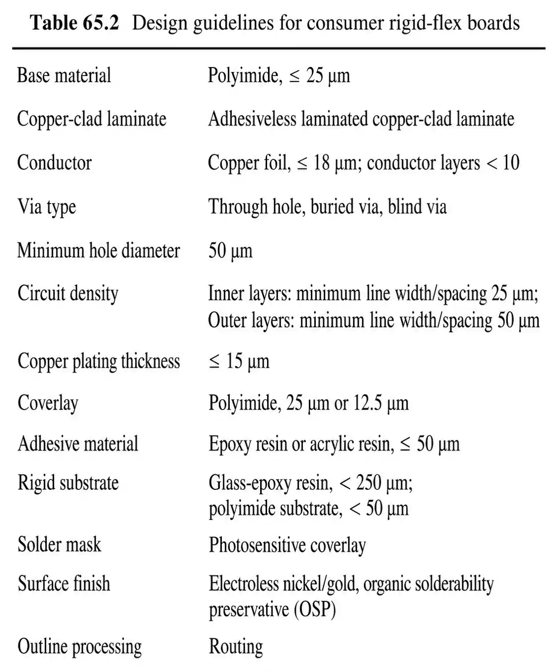
- line/space often pushed below 75 um when HDI or build-up is in play
- blind microvias commonly below 150 um diameter
- dense SMT and sometimes flip-chip style attach in rigid zones
- flex tails that still carry meaningful current--thin does not erase I^2R or heating
Rigid vs flex role split
| Zone | What it should do | What fab rejects when misused |
|---|---|---|
| Rigid | Component mounting, dense SMT, local stiffness | Treating the whole part as "flex with pads" and omitting stiffener/coverlay intent |
| Flex | Fold, turn, cross-module interconnect | Dynamic hinge callouts on a static install-once stack with no bend drawing |
| Transition | Survive lamination and fold without crack | Coverlay openings, copper balance, and adhesive squeeze-out left unspecified |
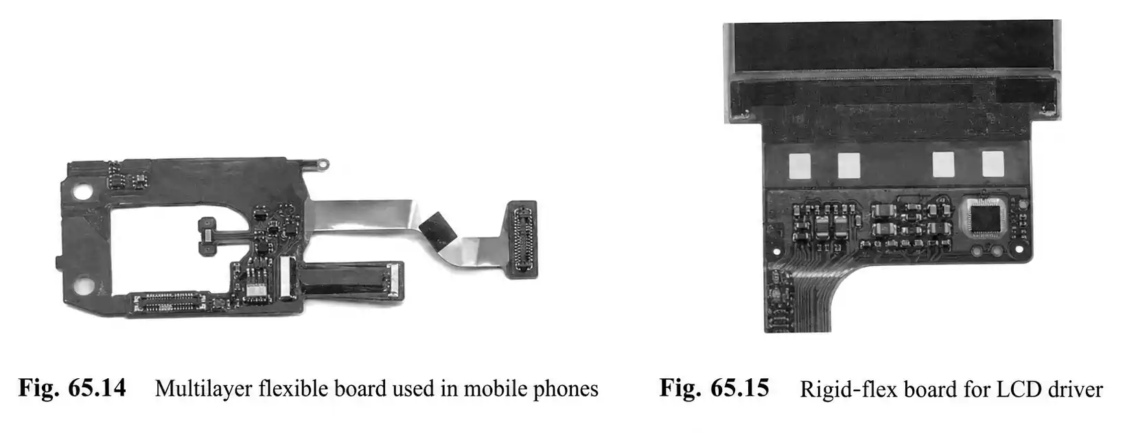
Smartphone display modules are a clean example: control ICs and dense passives on rigid islands, one flex path to glass (fine-pitch ACF), another into a board or FFC-style connector. The board is packaging the system--not winning a layer-count contest.
Density-cost levers the fab sees on your quote
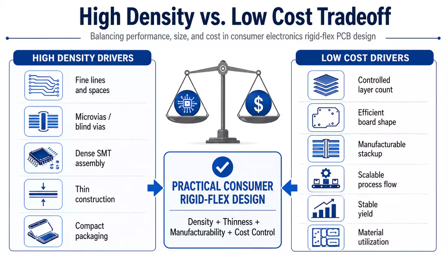
High density and low unit cost pull against each other. CAM reads your files for a short list of cost drivers long before anyone debates theory.
1. Layer count vs tighter line/space
Adding layers raises thickness, lamination risk, drill burden, and scrap exposure. If routing pitch is still relatively open (for example still above about 100 um), tightening line/space inside a manufacturable window often beats adding layers. Consumer programs usually try to stay at or under about 10 conductor layers unless the product envelope forces otherwise.
2. Thin materials are not free
Polyimide below 50 um helps fit thin devices and thinner SMT islands, but dimensional stability gets harder through bake, lamination, and laser steps. Thin is a product requirement, not a coupon for lower price. Expect tighter compensation control and more yield sensitivity--price the process window, not only the film datasheet.
3. Hole-wall copper can be lighter--within a stated reliability window
Consumer builds can often run lighter PTH copper than aerospace when life and environment allow it. That does not mean "plate as little as possible." Once copper thins, drill quality, desmear/plasma, and plating uniformity dominate escapes. Put the acceptance intent in the RFQ instead of hoping the fab guesses.
4. Re-engineer the rigid area for thickness
CE stacks sometimes replace thick glass-epoxy outer constructions with polyimide-forward or adhesiveless approaches, or laminate foil plus a bonding sheet onto a flex core, to keep rigid SMT zones thin while still mounting parts. A carefully optimized 6-layer style construction can land rigid areas well under half a millimeter when the product needs it--but only with a locked stack sketch, not a verbal "make it thinner."
5. Board outline is a cost variable
Irregular, fragmented outlines kill panel utilization. A compact rectangle or near-rectangular envelope improves material use, scoring/routing flow, and unit cost. Odd "jigsaw" shapes may be mechanically necessary; if they are not, they are a self-inflicted NRE and yield tax.
6. Bookbinder is usually the wrong volume lever
Bookbinder stagger (progressively longer outer flex lengths) helps short multilayer bends, but tooling and throughput often miss CE volume economics. Prefer it when bend reliability is the bottleneck and volume can absorb the process; do not paste it into a cost-first phone or wearable RFQ as decoration.
Process windows that protect yield
Density is only useful if the panel yields. These are the shop-floor controls that show up when CE rigid-flex either ships or scrapes.
Microvia / sequential build-up. Buried vias and outer microvias free routing without reflexive layer adds. Opening copper windows for CO2 laser drilling supports high via counts at production rates; quoting "HDI" without via map and capture-pad rules just invites clarification loops.
Adhesiveless materials. Cast or laminated adhesiveless constructions often reduce smear, survive repeated heat, and keep thickness down--useful when the stack sees multiple laser and lamination cycles.
Desmear / plasma. Even with lighter hole-wall copper, reliability still rides on hole preparation. Acrylic adhesive systems in particular may need plasma where conventional permanganate desmear swells the material. Name the construction so CAM picks a real process path.
RTR vs sheet. Inner layers without holes can use roll-to-roll efficiently. Inner layers with holes demand tight dimensional control; otherwise RTR becomes a scrap machine.
Profile method. High-volume punching or stamping can beat CNC routing on unit cost, but poor die geometry notches flex edges. Soft flex edges need explicit edge-quality notes; otherwise first-article "looks fine" dies later in fold testing.
Coverlay, stiffener, and selective openings. State coverlay vs flexible solder mask, stiffener material/thickness/keep-outs, PSA vs thermal bond, and whether stiffeners stop before the bend. Missing stiffener drawings are a common reject or endless EQ.
Dimensional control = yield. Thin flex moves through thermal cycles. Anticipated scale factors, panel size choice, and copper balance matter more than a single "IPC class" checkbox. Many CE rigid-flex cost overruns are yield problems dressed up as material price.
What fab DFM actually asks (and rejects)
Before you compare China quotes on schedule alone, expect CAM to ask for:
- Stackup sketch with rigid/flex layer map and total thickness targets
- Bend drawing: static vs dynamic, radius, direction, cycle count if dynamic
- Coverlay/stiffener openings and adhesive type
- Via strategy: through / blind / buried, laser size, capture pads
- Preferred outline for panelization, or acknowledgment that irregular outline is mandatory
- Surface finish and any selective hard-gold or soft-gold zones
- Acceptance class and whether microsection is required on first article
Common rejects or holds: dynamic flex called out with no bend life, coverlay openings into the bend with brittle finishes, bookbinder notes without stagger detail, outlines that leave unusable panel waste with no mechanical justification, and "as thin as possible" with no dimensional tolerance.
Closing the loop: system value, not board vanity
The smartphone display-module pattern shows why CE rigid-flex wins when it is specified honestly: control circuitry, dense SMT, display interconnect, and folded routing land in one structure. Fewer connectors, fewer discrete FPCs, simpler final assembly, tighter mechanical fit. That system-level saving usually matters more than winning a one-board price fight against an overbuilt aero-style stack that never belonged in the product.
XFPCB quotes consumer rigid-flex from the same shop-floor filters used on panelization, laser microvia, coverlay/stiffener, and dimensional yield--not from a copied high-reliability checklist. Send Gerbers, stackup, bend drawings, and volume intent so the NRE and unit price reflect the product you are actually shipping.