
Procurement teams usually meet connected SMD pads as an AOI scrap spike, not as a layout theory debate. A same-net copper pour that "looks fine" in CAD can still leave SPI volume looking normal while reflow pulls paste onto exposed copper, then AOI flags bridges, starved fillets, skewed 0402s, or tombstones that never appeared on a hand-soldered prototype.
For overseas buyers evaluating China PCBA quotes, the issue is process ownership: who catches merged solderable areas in DFM, how stencil apertures are drawn when copper is continuous, and what scrap language appears on the traveler when mask dams are missing. This article starts from that yield escape, separates electrical nets from solderable area, maps defect modes in buyer inspection language, then lists what CAM and SMT ask for in footprints--without an FAQ pad at the end.
When AOI scrap reveals a footprint problem
A recent mid-volume panel run illustrates the pattern. Paste print SPI passed aperture-to-aperture volume checks. Placement was within library offsets. After reflow, AOI scrap concentrated on a dense power-rail cluster: adjacent same-net pads sharing one large mask opening, plus one 0603 capacitor pad opened into a ground pour with no dam. Operators saw bridges between fine features, dull incomplete fillets where solder had wicked onto pour copper, and a handful of upright passives.
Electrical netlist was correct. Continuity tests on scrap boards still showed shorts that "should" be allowed on the same net--yet IPC workmanship and customer AOI criteria failed the lot. Rework cost and schedule slip belonged to the footprint and mask definition, not to a mysterious oven recipe.
Buyer takeaway: same-net does not mean same solderable pool. If your RFQ never asks for solder-mask dam review or pad individuality checks, two factories can quote the same Gerbers and deliver very different first-pass yield.
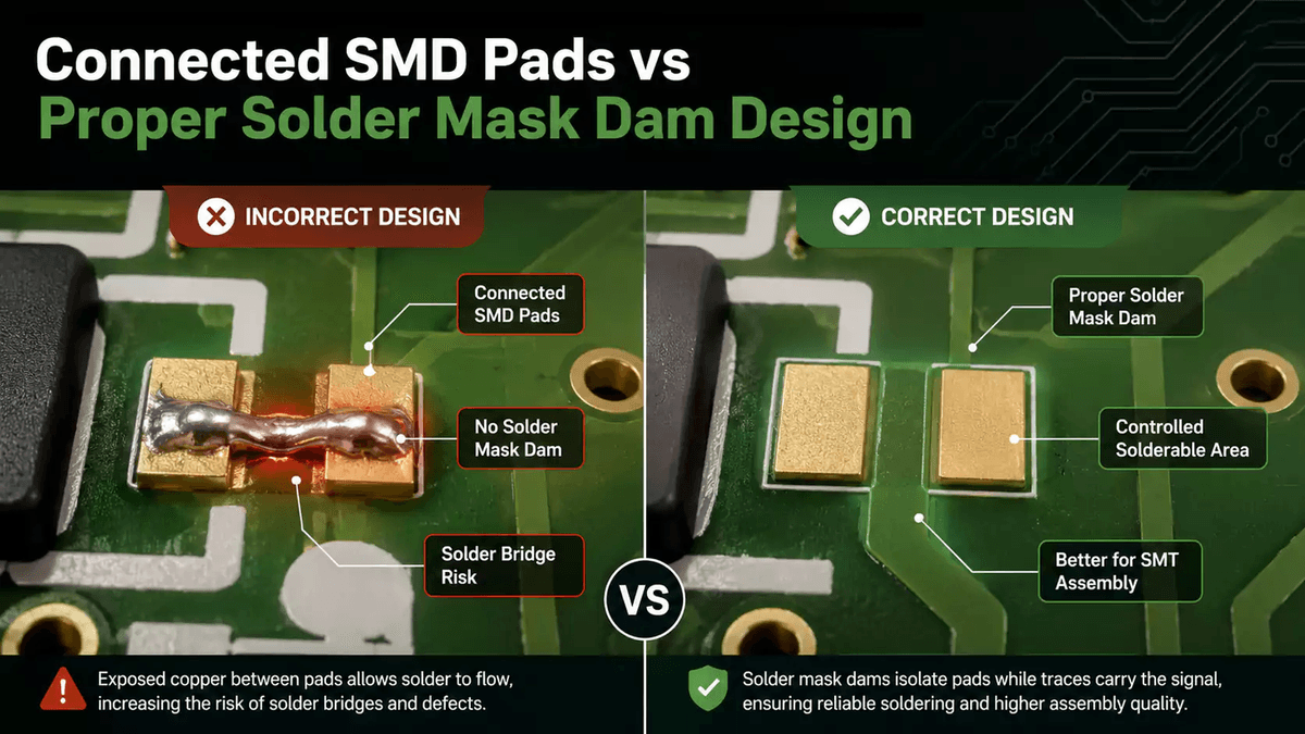
Electrical connection is not the solderable area
Layout tools make it easy to confuse continuity with wetting surface.
- Electrical connection: copper (trace, pour, via) ties points on one net so the circuit functions.
- Solderable area: copper the solder mask leaves open so molten solder can wet, spread, and form a joint under stencil-defined paste volume.
Good practice keeps those ideas separate. Connect same-net pads with a masked trace or internal plane. Keep each SMD land as its own controlled opening so paste stays where SPI measured it and surface tension centers the part.
When designers open one continuous copper shape across two lands, a pad plus pour, or a pad plus uncovered via entry, they enlarge the solderable area without changing the net. Stencil paste then has a larger wettable playground. During reflow the solder seeks that copper; joint volume, wetting time, and pull forces stop matching the library assumption.
Factory language for buyers:
| Concept | What it controls on the line |
|---|---|
| Net / continuity | ICT, flying probe, functional pass |
| Mask opening | Where solder is allowed to wet |
| Stencil aperture | Paste volume before reflow |
| Mask dam | Barrier that keeps molten solder from neighboring copper |
SPI can only police what the stencil prints. It cannot stop solder from leaving a pad onto adjacent exposed copper once the alloy melts. That is why connected SMD pads often look like "mysterious" post-reflow defects after a clean SPI report.
Defect modes in buyer inspection language
Connected pads rarely produce one neat failure mode. Scrap tickets usually mix the following--use this wording when you write AOI criteria or dispute first-article photos.
Bridges and unintended fillets
AOI may call bridge, short, or excess solder between pads or from pad to pour. Even on the same net, many customer specs still reject bridging as a workmanship fail, and dense areas can create solder that later cracks or complicates conformal coating and cleaning. Fine-pitch ICs and tight passive clusters are highest risk when dams disappear.
Starvation, incomplete wetting, weak joints
Opposite problem: solder drains onto large exposed copper, vias, or uncovered traces, leaving the terminal with a thin or incomplete fillet. AOI may flag insufficient solder, poor wetting, or open risk. Boards can still beep continuity and fail later under vibration or thermal cycling--classic escape if you only sample functional test.
Tombstoning on small two-terminal parts
0402/0603 (and smaller) resistors and capacitors stand up when one end wets earlier or with more pull than the other. Connected or asymmetric copper--one pad into a pour, the other on a thin trace--changes thermal mass and wetting timing. AOI reports missing, tombstone, or vertical component. Yield impact is immediate and obvious on the traveler.
Shift, skew, and float
Not every imbalance becomes a tombstone. Parts can rotate, slide, or sit with uneven fillets. Buyers see AOI skew/offset fails or borderline joints that pass electricals but fail cosmetic Class 2/3 criteria. Root cause is often unbalanced solderable geometry, not a bad nozzle alone.
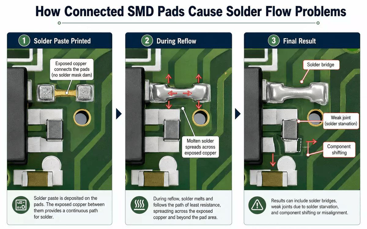
Hand-solder prototypes hide these modes: a technician adds or removes solder and nudges parts. Reflow does not. Once paste volume is fixed and copper is open, wetting physics runs the show across the whole panel.
Copper pours and vias that trap solder
Two layout habits amplify connected-pad scrap more than any other.
Large copper pours acting as heat sinks and solder lakes. A pad opened into ground or power copper heats differently from a pad on a thin trace. Heat-sink effect delays or advances melt timing; the open pour also gives solder a path to leave the joint. Thermal reliefs and mask-covered connections keep electrical attachment without turning the pour into one giant land.
Vias near pads and open via-in-pad. When a via sits inside the mask opening or too close without a dam, solder can wick into the barrel (solder escape). Joints look starved after reflow; BGA/QFN and small passives are common victims. If via-in-pad is required for density or thermal reasons, filled and capped (or plated-over) vias belong in the fab notes--open VIP is an assembly risk, not a free routing trick.
DFM questions worth putting on the quote checklist:
- Are adjacent SMD openings separated by a manufacturable mask dam for this fab's capability?
- Does any passive pad share a continuous opening with pour copper or a via?
- Are VIP features filled/capped where paste will print?
- Did CAM flag merged apertures or oversized mask openings against the stencil plan?
What CAM and SMT ask for in footprints
Before the first panel, footprint and mask data should answer shop-floor questions--not only pass a netlist ERC.
- One land, one controlled opening -- Library pads stay individual. Same-net ties use covered copper, not a merged copper island in the mask layer.
- Mask dams sized to fab capability -- Ask the fabricator for minimum dam width at your copper weight and mask process; do not assume CAD "minimum" equals yieldable.
- Stencil apertures drawn to the pad, not the pour -- Aperture design assumes discrete lands. Merged copper forces engineering judgment, extra review time, and yield risk.
- Thermal symmetry on small passives -- Both ends of 0402/0603 (and below) should see similar copper attachment and mask definition unless you deliberately accept tombstone risk.
- Via policy in the fab notes -- Keep open vias out of paste-print zones; specify fill/cap when VIP is mandatory.
- DFM feedback loop -- Send Gerbers, paste layer (or aperture drawing), and assembly notes early. A factory that returns clear mask-dam and VIP comments before stencil cutting is protecting your first-pass yield.
Prototype boards that "worked" on a hot iron are not evidence that the footprint is SMT-ready. Ask for SPI+AOI evidence on the first production panel, not only a power-on photo.
Closing
Connected SMD pads can be electrically correct and still destroy SMT yield. Molten solder follows exposed copper; without mask dams and individual lands, paste volume leaves the intended joint, AOI records bridges or starvation, and small passives tombstone or skew. Large pours and nearby open vias make the escape worse. Lock pad individuality, manufacturable dams, stencil-to-pad alignment, and via treatment into DFM before you compare China PCBA prices on schedule alone.
XFPCB reviews PCB fabrication and SMT footprints with the same shop-floor filters used on stencil, SPI, and AOI: discrete solderable areas, mask separation, and clear VIP notes. Send Gerbers, stackup, paste/aperture data, and your AOI acceptance class so the quote reflects real DFM risk--not a CAD net that happens to be continuous.