
Procurement teams rarely see Conductive Anodic Filament (CAF) on a first-article electrical test. Boards can pass continuity, hipot where specified, and early burn-in, then fail months or years later with intermittent leakage, unexplained resets, or a hard short between nets that never touched on the artwork. For overseas buyers sourcing multilayer and HDI boards from China fabs, CAF is a latent reliability risk you manage in the RFQ--not a defect you expect AOI to catch on finished panels.
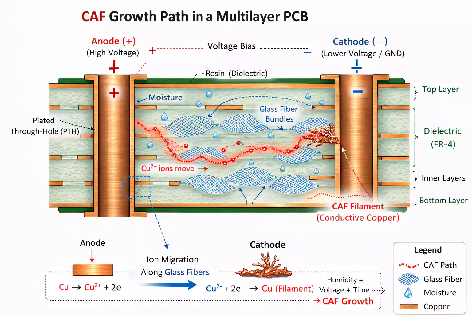
Conductive Anodic Filament (CAF) is an internal electrochemical failure mode: copper ions migrate through the laminate along glass/resin interfaces under moisture and DC bias until a conductive filament bridges conductors. This article starts with buyer risk and RFQ language, then explains the mechanism in plain terms, translates layout rules into fab notes and spacing tables, and lists material, process, and qualification questions you can ask without inventing certificate numbers.
Buyer risk first: why CAF belongs on the RFQ
Treat CAF like impedance or Tg--something you lock when humidity, voltage, lifetime, or via density make field failures expensive. If those drivers are absent, generic FR-4 and minimum drill-to-copper may be enough. If they are present, "cheapest stackup" quotes are not comparable.
RFQ checklist mindset (copy into fab notes)
Ask China fab partners to answer in writing before tooling:
- Named laminate family and whether a CAF-resistant grade is required or preferred (brand/type on the stackup drawing--not "equivalent FR-4")
- Minimum drill-to-copper and opposite-polarity via spacing you want as reliability rules, not only CAM minimums
- Bake / moisture-control steps before lamination or after moisture exposure (process description, not a marketing claim)
- Ionic cleanliness / contamination control expectations for the bare board process when your program cares about electrochemical migration
- Whether CAF or insulation-resistance style testing is in scope for coupons or qualification lots (only if your design authority requires it)
- Change control: no silent material swaps when CAF or humidity life is part of the reliability case
Comparable quotes name materials, spacing rules, and test deliverables. Vague "high reliability" language does not.
What CAF is, and why it fails late
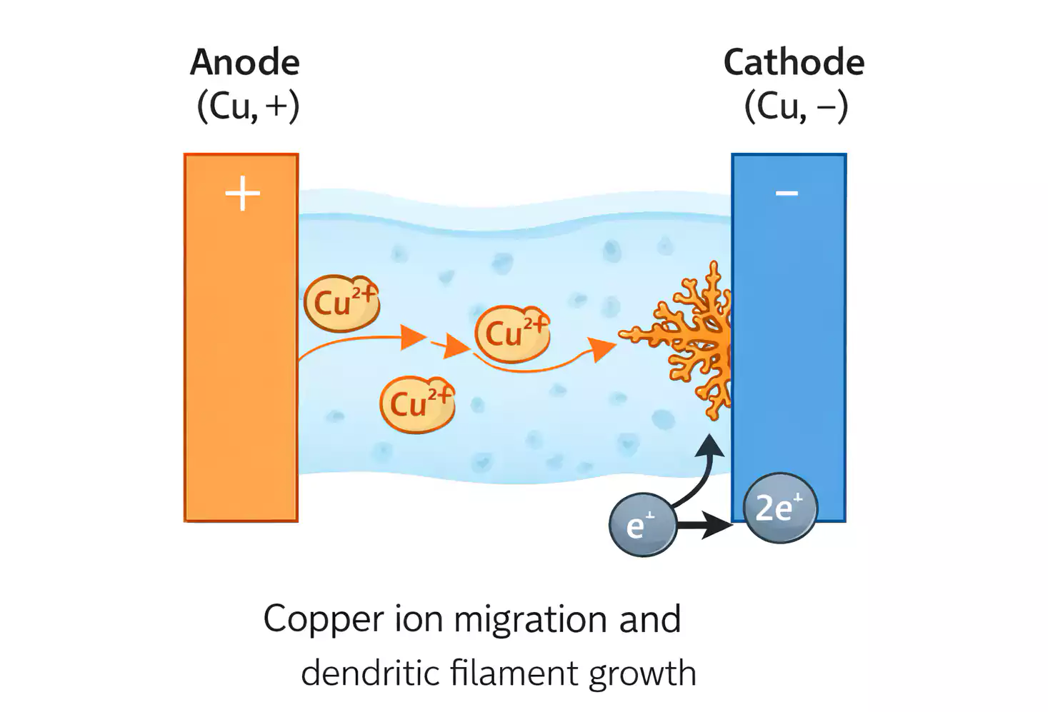
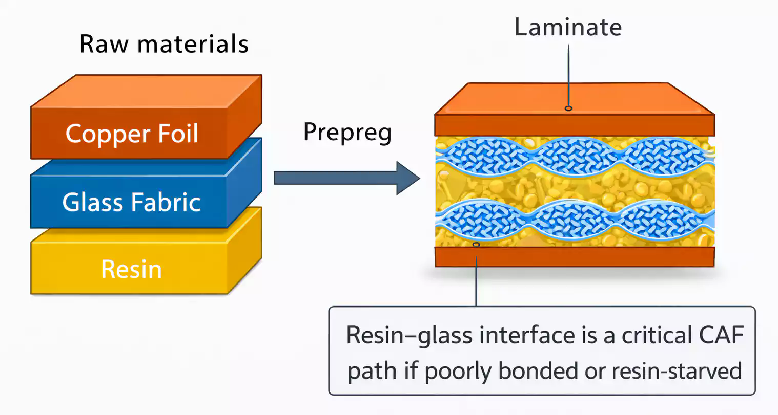
CAF grows inside the dielectric, typically along the glass-fiber / resin interface, not as a visible surface dendrite. Moisture absorbed into the board provides an ionic pathway. A sustained DC voltage bias dissolves copper at the anode; copper ions migrate along susceptible pathways; metal deposits toward the cathode and eventually forms a filament. Leakage rises first; a hard short can follow.
Late failure is the point: early electrical test may see open dielectric paths that only become conductive after humidity soak, bias hours, and micro-pathways open from resin voids, drill damage, or glass/resin weak bonds. That is why lab prototypes can look clean while field units in humid or condensed environments degrade later.
The three conditions (remember the triad)
CAF needs all three at once:
- Moisture in or on the dielectric pathway
- DC bias between conductors at different potential
- A susceptible material/path geometry (glass/resin interface, voids, microcracks, resin-poor zones, aggressive via proximity)
Remove or weaken any one condition and risk drops sharply. Buyers cannot "inspect CAF out" of a shipped board the way they catch a missing solder fillet; they reduce probability through design rules, laminate choice, and fab process discipline.
When a project should take CAF seriously
Prioritize CAF controls when several of these apply:
- High humidity, condensation, or outdoor/industrial moisture exposure
- Long product life (multi-year automotive, telecom, industrial, medical, infrastructure)
- Sustained DC voltage differences between adjacent nets or via barrels
- Dense via fields, thin dielectrics, HDI sequential build-up, or tight drill-to-copper
- Safety, uptime, or warranty cost that makes intermittent shorts unacceptable
Consumer gadgets with short life and mild environments often accept commodity spacing. Automotive ECUs, outdoor radios, dense power-digital boards, and high-layer compute/telecom hardware usually should not.
Layout rules buyers should turn into spacing tables and fab notes
Most CAF mitigation starts at layout, but overseas buyers need DFM translation: what CAM will enforce, what to put on the drawing, and what to pay for beyond the absolute fab minimum.
1. Increase spacing on opposite-polarity conductors
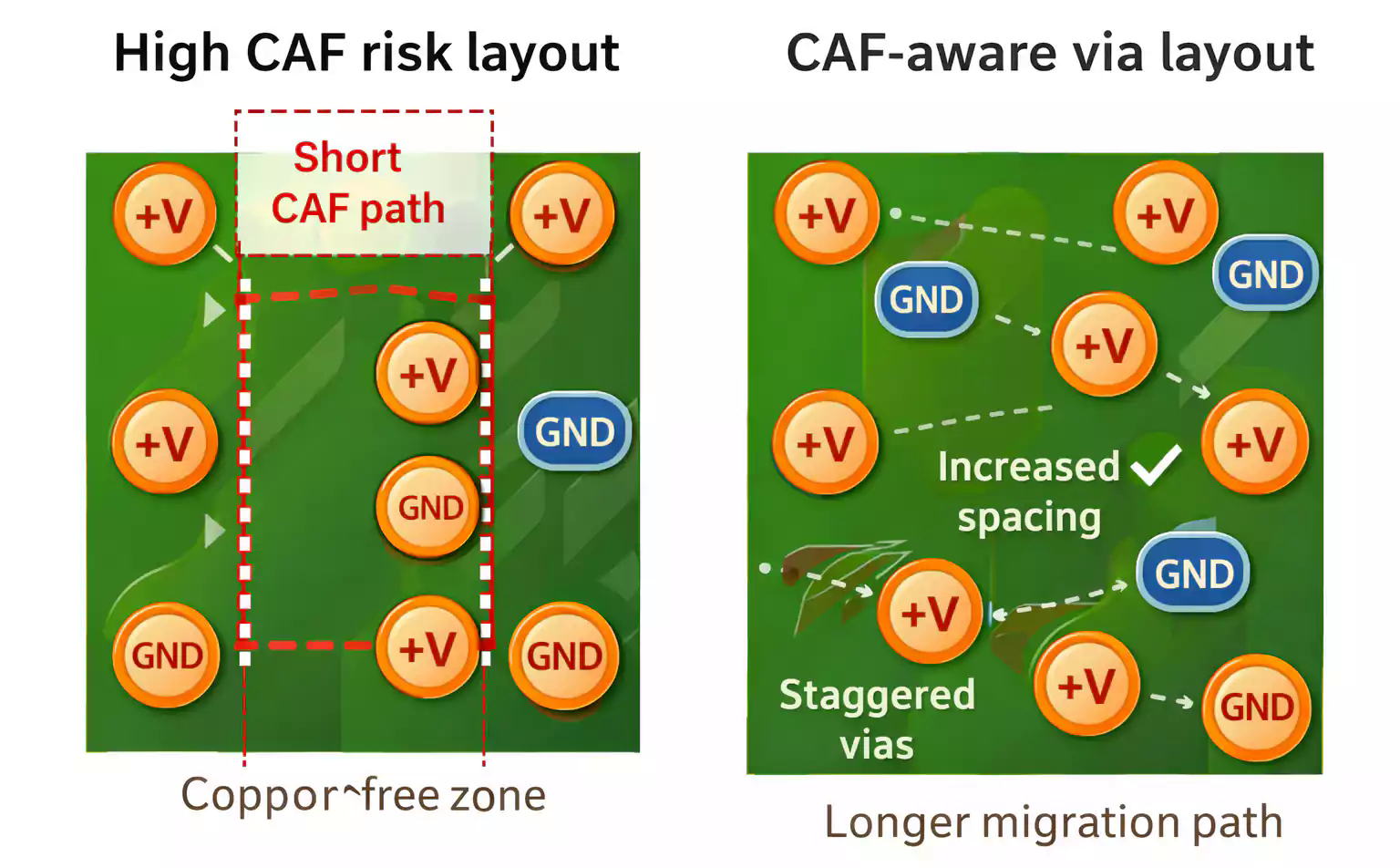
Longer paths and weaker electric fields slow ion migration. Call out extra margin for via-to-via, trace-to-via, and plane-split edges--especially on inner layers where glass weave pathways matter. Put numbers in a spacing table: "minimum drill-to-copper X mm on opposite-polarity nets" and "add Y mm reliability margin vs fab min" when your reliability case requires it.
2. Remove orphan pads and useless inner copper islands
Unused pads and floating copper create resin-starved zones and moisture traps. Clean non-functional pads from internal layers unless the fabricator needs a minimal annulus for drill support--then keep the smallest supported feature, not a large island.
3. Stagger opposite-polarity vias (~45 degrees or pitch offset)
Straight-line anode-cathode via pairs give ions a short geometric path. Rotate or offset via columns so migration must follow a longer, more tortuous glass/resin route. Document "no collinear opposite-polarity via pairs under Z mm" in DFM notes when density allows.
4. Avoid long parallel rows of opposite-polarity vias
Via barrels are vertical conductors; long parallel opposite-polarity rows multiply field and path opportunities. Break rows, increase pitch, or offset columns. Treat drill-to-copper as a reliability rule on biased nets, not only a drill-breakout manufacturability limit.
5. Break up dense via farms where possible
Tight via clusters under BGAs or connectors can create microcrack and resin-depletion zones plus high local fields. Prefer staged fanout, local keepouts between different potentials, and avoid packing unrelated power/return/signal vias into one capillary farm when density is optional.
6. Use teardrops on pad and via transitions
Teardrops reduce stress concentration at copper-to-drill junctions and help limit microcracks that later hold moisture. Low cost on most CAM flows; worth calling out on high-reliability or dense breakout boards.
Buyer DFM translation (what to put on the drawing)
| Intent | Example fab-note language (adapt numbers to your design) |
|---|---|
| Spacing | Opposite-polarity via drill-to-copper min XX mm (YY mm above fab min) |
| Orphans | Remove non-functional pads on inner layers except fabricator-approved drill support |
| Stagger | Offset opposite-polarity via columns; avoid straight-line pairs under XX mm |
| Via farms | Max cluster density / keepout between nets at different potential as shown |
| Teardrops | Apply teardrops on SMT pads and vias unless impedance geometry forbids |
| Material | Laminate type locked; CAF-resistant grade required/preferred as named |
Do not paste another company's numbers blindly. Set margins from voltage, humidity class, dielectric thickness, and your fabricator's process capability.
Materials and China fab process questions that matter
CAF is not only a layout problem. Laminate chemistry, glass weave, resin fill, drilling, desmear, cleanliness, and moisture control decide whether weak pathways exist after the board is built.
Laminate and stackup
Ask for the actual grade on the traveler, not "FR-4 equivalent." CAF-resistant formulations exist in several supplier families; what matters is a named type your design authority accepts, with documented Tg, CTI if relevant, and any CAF performance claims backed by supplier data sheets--not a generic slogan. Lock approved alternates in writing if second sources are allowed.
Cleanliness and ionic contamination
Electrochemical migration needs ions and moisture. Buyers who care about CAF or ECM should ask how the fab controls process contamination, rinse quality, and handling--and whether bare-board ionic cleanliness measurements are available when the program requires them. Align expectations with your reliability standard; do not invent a cert code the factory does not hold.
Drilling, desmear, and hole-wall quality
Rough holes, cracks, and incomplete smear removal create capillary paths. Ask how the fab qualifies drill and desmear for your aspect ratio and material, and whether microsections are available on first articles for critical builds.
Bake and moisture discipline
Moisture is one of the three CAF conditions. Reasonable questions: pre-lamination dry-out practice, bake after wet processes when required, and packaging/desiccant for multilayer shipments to humid destinations. Expect a process description, not a fake "CAF certified" stamp.
What XFPCB can support without fake certificates
XFPCB builds multilayer, HDI, and high-reliability boards when drawings name materials, spacing, and acceptance criteria. We can discuss CAF-resistant laminate options, stackup DFM, drill-to-copper capability, bake/moisture handling, and coupon or insulation-resistance style tests when your specification requires them. We will not invent XFPCB CAF certificate numbers or claim every FR-4 panel is CAF-proof. Clear notes make quotes honest and comparable.
Tests and qualification buyers can request
Do not confuse bare-board process capability with equipment-level humidity qualification. Useful asks include:
- Supplier CAF or insulation-resistance data for the named laminate (data sheet or supplier report)
- First-article microsections on via/dielectric quality for dense or high-voltage designs
- Program-defined CAF / SIR / humidity-bias coupon testing when your design authority or customer requires it--state the method and accept/reject criteria on the PO
- Lot traceability and material certificates for the locked grade
Avoid RFQ lines like "must be CAF certified by XFPCB" with no method. State the test standard or customer method, sample size, and deliverable report instead.
Practical takeaway
CAF is a slow internal copper filament driven by moisture, DC bias, and a weak glass/resin pathway. It passes early tests and then creates leakage or shorts in the field. Buyers prevent it by putting risk on the RFQ: lock laminate, write opposite-polarity spacing and via stagger rules into fab notes, clean orphan copper, and ask China fabs for bake, cleanliness, drill/desmear, and any real coupon testing your program needs--without brochure-only "CAF free" claims. Good layout cuts probability; disciplined materials and fabrication close the remaining gap.