
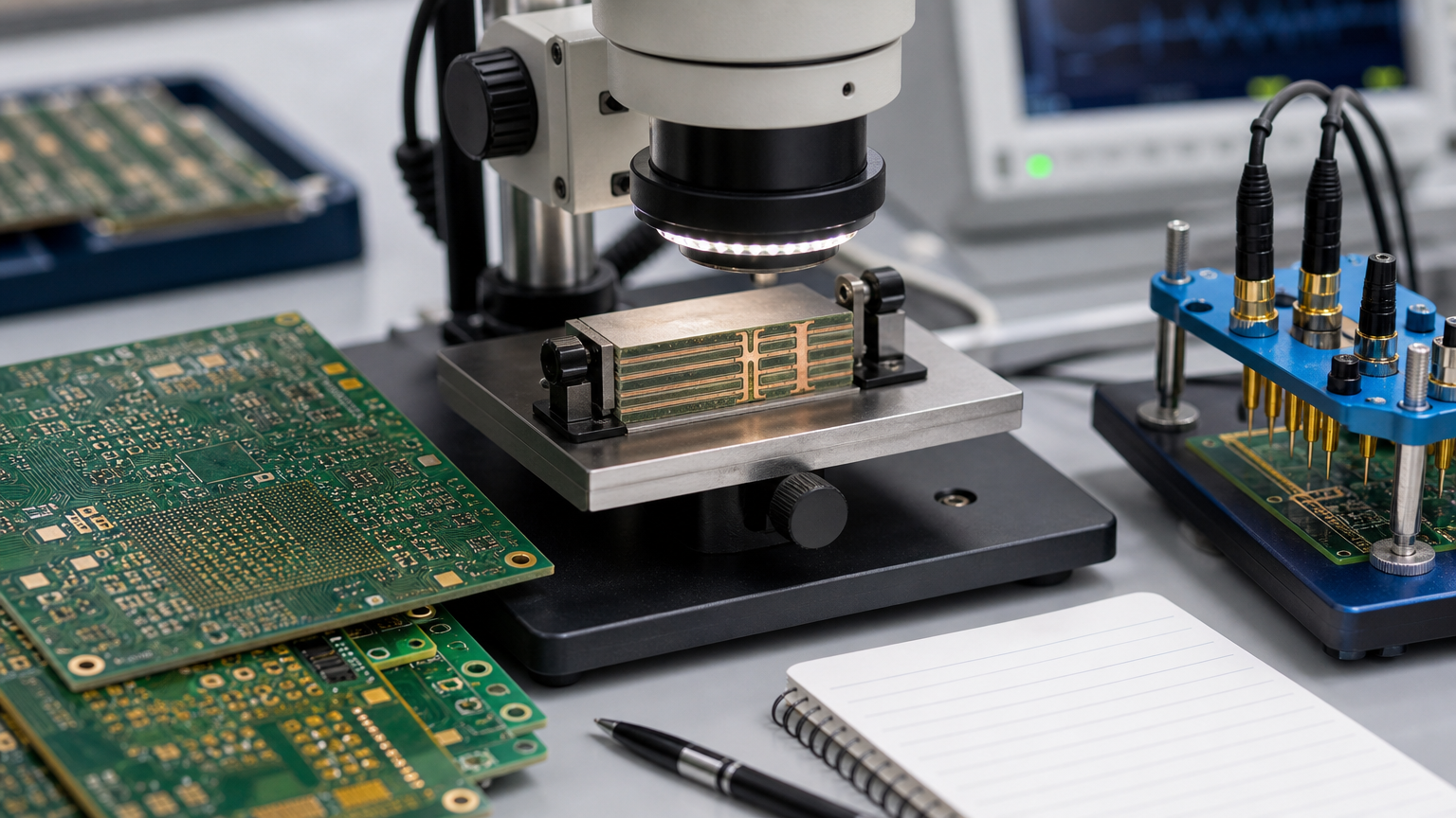
Press-fit connectors and thick high-layer panels turn backplane work into a mechanical manufacturing problem as much as a routing problem. If hole tolerance, aspect-ratio plating, or warpage drift, daughter cards will not seat—and no amount of SerDes equalization fixes a bent slot.
A backplane distributes multi-gigabit differential channels, power, and ground across a chassis while providing the structural backbone for modules. Passive backplanes are mostly interconnect; active or hybrid versions add drivers, management, or power circuitry and therefore assembly test scope. This guide focuses on layout and manufacturing limits overseas buyers should lock before RFQ, not a generic "what is a backplane" brochure.
Backplane versus motherboard (and why buyers mix them up)
A motherboard hosts CPUs, memory, and much of the system logic. A backplane is judged on connector geometry, channel continuity across long paths, copper current density, and thick-board yield. Size and thickness drive lamination, imaging, drilling, and handling difficulty beyond a typical eight-layer logic card.
| Topic | Typical function board | Backplane |
|---|---|---|
| Main role | Compute / control function | Module interconnect + structure |
| Size / thickness | Smaller, thinner | Often larger and thicker |
| Connectors | Limited | Dense slots / press-fit fields |
| Design focus | Components + local SI | Channels, PDN, mechanics, yield |
| Fab stress | Standard multilayer | Registration, aspect ratio, warpage, hole tolerance |
Define module count, data rates, voltage/current per slot, connector family, and chassis constraints before stackup arguments begin. Late connector swaps rewrite both signal-integrity assumptions and drill programs.
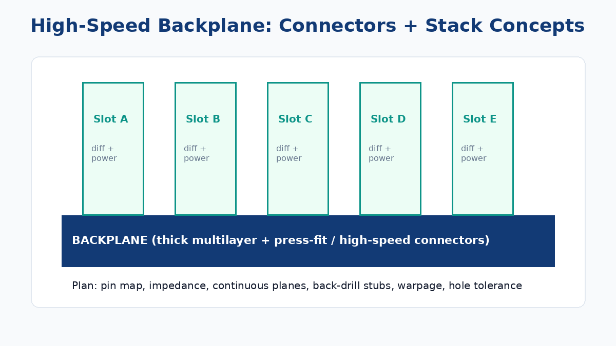
Passive, active, and hybrid—scope that changes the quote
Passive backplanes primarily wire connectors together. Assembly may be connector-heavy and still non-trivial, but IC test scope is limited.
Active backplanes add buffers, management controllers, or power devices. That means SMT, firmware bring-up hooks, and different failure analysis.
Hybrid designs sit between: mostly interconnect with limited active housekeeping.
Buyers should state which type they are quoting. A "backplane PCB" line item without that distinction invites underpriced assembly assumptions.
Layout priorities that survive CAM
Keep high-speed pairs referenced to continuous planes; avoid routing across splits. Match differential length and geometry deliberately, and treat every layer transition as a discontinuity to minimize. Place ground pins strategically in connector pin fields to contain return loops.
Power distribution needs plane weight, via count, and connector pin allocation sized for voltage drop and heat. Weak PDN design shows up as slot-dependent brownouts and EMI complaints that look like "signal" problems.
EMI/EMC basics still apply on large panels: short returns, edge clearance for aggressive clocks, separation of noisy and quiet nets, and connector pin maps that do not force huge loops. Backplanes magnify mistakes because channels are long and connectors are repeated.
Practical routing habits that CAM engineers recognize as serious:
- Lock target impedances (for example 85 ohm or 100 ohm differential—use your standard) in fab notes with reference layer callouts.
- Prefer broadside or edge-coupled pair geometries consistently; do not mix styles casually on one channel.
- Minimize via count on multi-gigabit lanes; when vias are required, plan stub control early.
- Keep pair phase/length budgets honest against connector skew and breakout.
- Do not starve ground pins beside fast pairs in the connector map to "save pins" for low-speed GPIO.
Materials: high-Tg FR-4 versus lower-Df—choose by length and rate
Industrial chassis often run high-Tg FR-4 successfully. Longer, faster channels may need lower-Df materials on selected layers. Choose based on length, rate, temperature, and cost—not a blanket ultra-low-loss mandate.
Material properties buyers should see on the stackup, not only in a sales slide:
- Tg — thermal stability through assembly and operation
- CTE — plated hole reliability through thermal cycles
- Dk / Df — impedance and loss over backplane lengths
- Dimensional stability — multilayer registration on large panels
- Availability — exotic cores that delay every respin
Hybrid stackups (standard loss inner power, lower-Df outer signal) can be valid. They also need clear fab notes so CAM does not "simplify" your intent into one resin system.
Via stubs, back-drill, and thick-board reality
Thick boards make through-hole stubs painful. A plated through-hole that continues past the signal capture layer leaves a stub. At multi-gigabit rates, stubs contribute reflection, resonance, and insertion-loss structure that equalization may only partially hide.
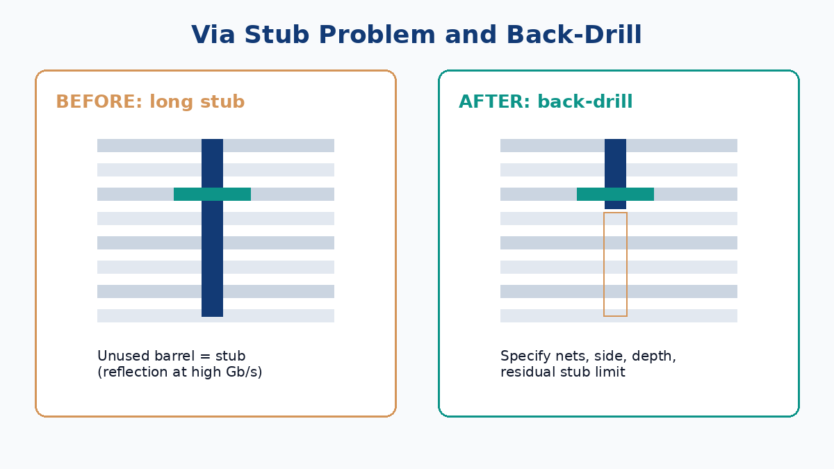
Back-drill callouts should be explicit in fab notes: nets (or via list), drill side, target depth / layers, and allowed residual stub with tolerance. Residual stub limits that the drill process cannot hold are not real limits—they are wishful documentation.
If the channel can use blind/buried structures or optimized layer exits instead of long stubs, evaluate that against yield and cost. Not every backplane needs every via back-drilled; the ones on the critical SerDes lanes usually do.
Manufacturing challenges to price honestly
Large panel size. Imaging, etching, and handling tolerances grow with dimension. Flatness and feature uniformity are harder to hold.
High layer count. Registration budgets shrink. Annular rings that looked safe in CAD become escapes when layer shift consumes margin.
Thick drilling. Smear, roughness, positional error, and tool wear rise. Drill quality feeds plating quality.
High aspect-ratio plating. Deep small holes challenge copper uniformity. Thin barrels that pass room-temperature ET can still crack in thermal cycling.
Press-fit hole tolerance. Press-fit connectors need tight finished-hole diameter control. Loose holes yield intermittent contact; tight holes yield insertion force problems and damaged pins.
Warpage. Unbalanced copper and asymmetric stackups bend thick panels. Warpage misaligns entire slot fields—mechanical failure first, electrical symptoms second.
Ask for capability evidence on board size, thickness, aspect ratio, press-fit hole tolerance, impedance coupons, and back-drill residual control before committing mechanical designs. A shop that cannot discuss residual stub capability on your thickness is not yet a backplane shop for your program.
Failure cases buyers should recognize early
Slot-dependent link training failures. Often a combination of stub resonance, connector pin map, and reference discontinuities—not "bad ICs" on one slot only.
Daughter cards that seat hard on one end of the chassis. Warpage or connector height stackup; measure boards, do not only reflow blame upstream.
Field opens after thermal cycles. High aspect-ratio vias with marginal plating; review cross-sections from first articles.
PDN collapse when multiple modules peak together. Plane copper and pin allocation undersized; SI tools will not save a power problem.
EMI failing only with all slots populated. Return path and cable/chassis bonding issues amplified by real load—plan ground strategy with full population in mind.
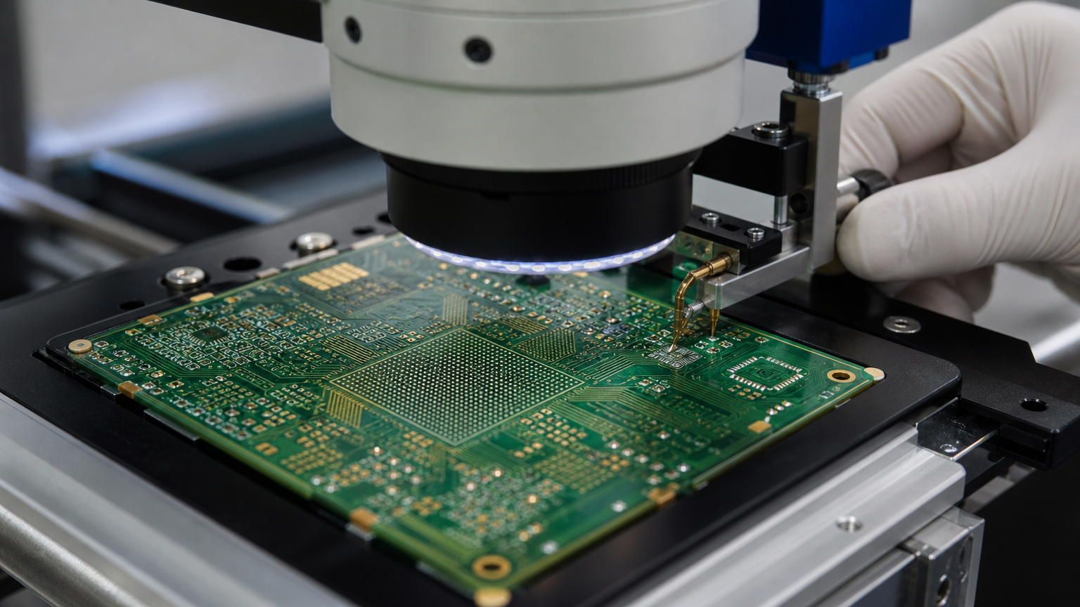
Connector selection notes that belong before routing
High-speed backplane connectors are not interchangeable footprints with different brand logos. Impedance, crosstalk, mating cycles, press-fit vs solder, and pin map conventions differ. Power pins and ground pins must be allocated with current and return quality in mind—not leftover after "all the GPIO is placed."
For press-fit, finished hole diameter, plating type, and board thickness interact. Changing thickness late can invalidate the connector's qualified hole window. For soldered connectors on active backplanes, thermal mass and wave/selective solder process constraints show up in assembly quotes.
If the chassis uses keyed slots or blind-mate guidance, mechanical drawings must drive PCB keep-outs early. Electrical CAD alone will not catch a stiffener that collides with a capacitor field on an active backplane.
What to put in a backplane RFQ package
Beyond ordinary Gerbers:
- Connector manufacturer drawings and finished-hole specs (especially press-fit)
- Stackup with impedance structures and material callouts
- Back-drill maps / via lists with residual stub limits
- Board thickness, copper weights, and warpage limits if the chassis demands them
- Surface finish compatible with press-fit and any SMT on active backplanes
- Test notes: bare-board ET coverage, and assembly test strategy if active
- Mechanical constraints: keep-outs, stiffeners, chassis mounting, slot pitch
Related capability discussions with XFPCB support usually start from multilayer impedance control and thick-board drilling limits—not from a layer-count slogan. Include connector drawings and back-drill maps when you request a quote so CAM risk is visible before metal is committed.
Closing discipline
Treat the backplane as a system mechanical part that happens to carry multi-gigabit electronics. Layout rules without manufacturable holes and flat panels are fiction. Manufacturing capability without controlled impedance and stub limits is also fiction. Programs that win write both into the same RFQ and refuse to compare quotes that omit them.