
Same-day conductive-ink prints solve a different problem than etched copper from a fab house. Confusing the two burns budget on consumables while still leaving you without solder mask, reliable multilayers, or controlled impedance for a customer release.
Desktop PCB printers deposit conductive ink or paste onto FR-1, FR-4, PET, or similar substrates, then cure or sinter traces. Some platforms add paste dispense and light reflow. They shine for education, early R&D iteration, and IP-sensitive bench work where uploading Gerbers is restricted. They do not replace a fabrication line when the board must meet electrical specifications, cosmetic standards, or volume.
This article is a buyer-and-lab-lead reality check: what printers do well, where fab houses remain mandatory, how to read printer specs without marketing fog, and a hybrid workflow that most serious teams eventually land on.
What a desktop PCB printer is (and is not)
A PCB printer—sometimes called a circuit board printer—builds functional conductive traces on a substrate. It is not a plastic 3D printer with a different filament. The output is an electrical circuit experiment, not an enclosure.
Typical workflow:
- Design in ECAD (KiCad, Altium, and similar).
- Export Gerbers (or the vendor's intermediate format).
- Import into printer software and set substrate / ink parameters.
- Deposit conductive ink through a fine nozzle (direct ink writing and related methods).
- Cure or sinter traces with controlled heat (or other vendor process).
- Optionally dispense solder paste and reflow on the same platform.
- Probe, fix, and iterate.
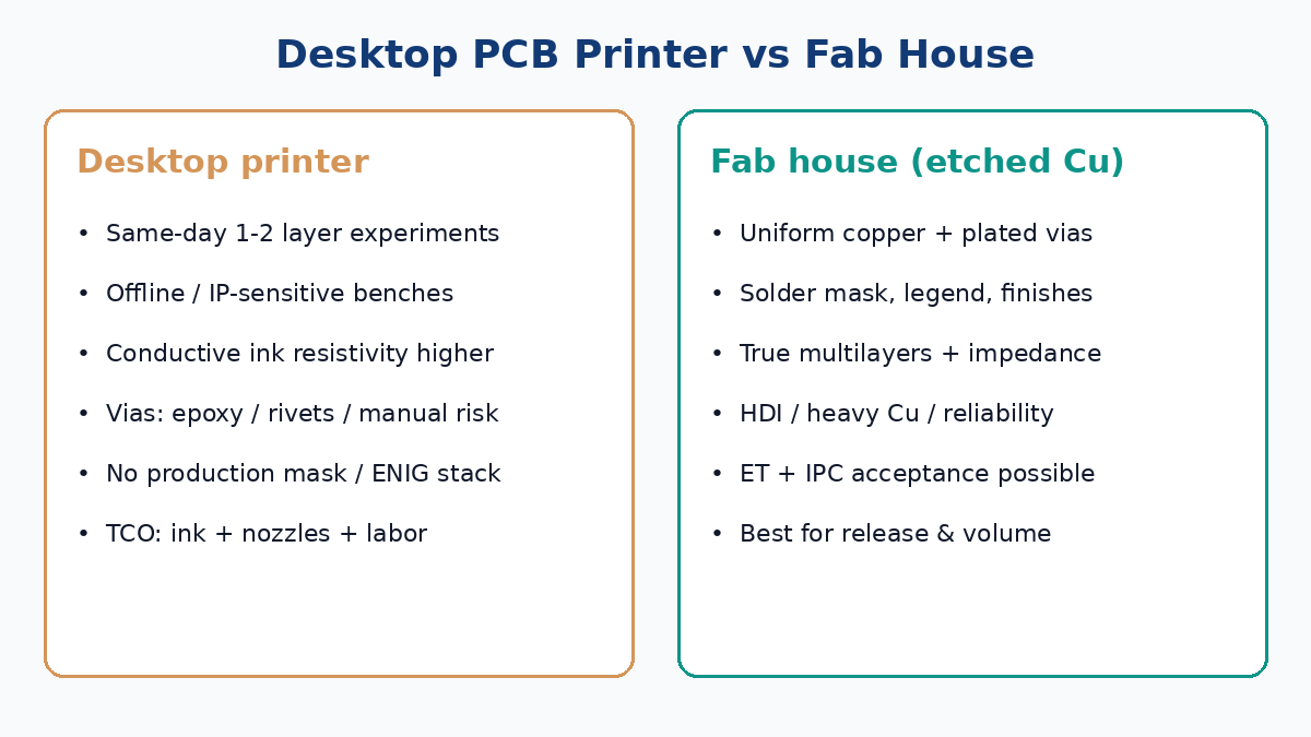
Through-hole strategies vary: conductive epoxy dots, tiny rivets, mechanical drills, or "avoid through-holes." Each adds manual risk compared with plated through-holes from a fab.
Where printers earn their keep
Hours instead of days for simple experiments. Single-sided and modest double-sided boards for sensor pinouts, LED matrices, and analog front-end ideas can move from CAD to a probe-able board before lunch—if the ink process is already dialed in.
Offline and IP-sensitive benches. Defense-adjacent labs, pre-patent skunkworks, and classrooms that cannot upload designs still need physical circuits. Keeping Gerbers off external networks is a legitimate requirement, not paranoia.
Unusual substrates. Research groups print on PET, polyimide films, paper experiments, and other carriers etching never targeted. That creativity is real. It is also usually research-grade, not IPC-class production.
Teaching and hiring filters. Students and new hires learn the difference between a netlist and a solder joint faster when iteration is cheap in time.
Where fab houses remain mandatory
Production copper thickness uniformity, plated vias, solder mask, legend, ENIG/HASL-class finishes, and true multilayer stackups still come from fabrication lines. Impedance-controlled differential pairs, HDI, heavy copper, and automotive or medical reliability stacks are outside desktop printer scope.
Printed traces typically show higher resistivity and less durable surfaces than etched copper. Oxidation behavior, abrasion resistance, and long-term contact reliability differ. Via strategies (conductive epoxy, rivets) add manual variation. Consumable ink cost and nozzle maintenance are real TCO lines that sticker price hides.
If a stakeholder asks whether a printer can "replace China fab capacity," the accurate answer is no. It can replace waiting for some early learning loops. Those are different sentences.
Buying criteria if you still need a printer
Treat listed resolution as a process capability to verify on your ink lot, not a guarantee stamped on every board.
Check at least:
- Minimum printable trace/space — hobby-class systems often land around the 100–150 µm neighborhood depending on ink and tuning; verify with a comb pattern, do not trust homepage crops.
- Supported substrates — FR-1, FR-4, Kapton, PET, textiles; curing temperature must not destroy the carrier.
- Ink resistivity and shelf life — conductivity, adhesion, and cartridge cost per useful board.
- Working area — maximum board size you will actually use.
- Gerber import quality — broken apertures and mis-scaled drills waste days.
- Through-hole method — epoxy, rivets, drill accessory, or none.
- Paste + reflow integration — valuable if you want one-stop tiny assemblies; still not a full SMT line.
- Vendor support and calibration burden — orphaned hardware with expired ink SKUs is a paperweight.
Entry systems commonly sit in the low thousands of USD; advanced multi-material tools climb much higher into five figures. Compare monthly iteration count against quick-turn fab pricing rather than against "feels cool in the lab."
TCO math that survives contact with accounting
Outsourced quick-turn prototypes for simple 2-layer boards can be inexpensive per panel relative to a printer's capital + ink + labor, especially when you only iterate a few times per quarter. Shipping and customs add calendar time, which is the printer's strongest counter-argument.
Ownership tends to win when:
- The team prints many iterations per month and operator time is already funded.
- Same-day learning unblocks a larger schedule (mechanical fit, connector pinout, bring-up sequencing).
- Designs cannot leave the building.
Ownership tends to lose when:
- Iterations are occasional.
- Boards need mask, controlled impedance, or more than trivial via structures.
- Nobody owns nozzle maintenance and ink inventory discipline.
A useful internal rule: if the printer is justified as "manufacturing," reject the justification. If it is justified as "instrumentation for learning," evaluate it like other lab instruments.
Common misunderstandings that create disappointment
"It prints multilayer like a fab." Some high-end systems can stack limited conductive/insulating prints. Complexity and reliability drop quickly. Do not promise four-layer production stackups from a bench printer.
"Resolution equals fab etch quality." Edge roughness, thickness uniformity, and via reliability are different physics. A narrow printed trace can still be a poor microwave or power path.
"We will add solder mask later somehow." Manual coatings exist for experiments. They are not a substitute for photoimageable mask registration on fine pitch.
"Double-sided alignment is free." Flipping, registering, and connecting layers is where many student and startup prints fail. Budget process time.
"Ink is a one-time cost." Cartridges, cleaning, failed prints, and recalibration dominate after the unboxing photo.
Hybrid workflow that most teams land on
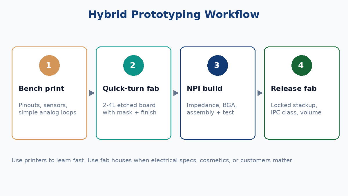
Print to learn pinouts, gain staging, and mechanical fit of simple circuits. Fabricate for anything that must meet electrical specifications, cosmetic standards, or customer-facing reliability.
A practical sequence:
- Bench print — prove connector pinouts, sensor orientation, and crude analog ideas.
- Quick-turn fab — 2–4 layer etched boards with mask and a real finish for bring-up that must look and behave like a product.
- NPI fab + assembly — lock stackup, impedance, and SMT process; add test coverage.
- Release fab — frozen documentation, IPC class, and volume planning.
Do not promise stakeholders that a printer replaces China or local fab capacity. Promise faster learning before you spend fab dollars—and then spend fab dollars when the design earns them.
Decision vignettes (so the meeting ends)
University lab, 30 students, weekly labs. A shared printer can be excellent. Pair it with a small fab budget for final project boards that need vias and mask.
Startup iterating a 6-layer impedance-controlled IoT hub. Buy fab turns. A printer will not teach you stackup loss or BGA escape reality.
Defense contractor evaluating antenna feed ideas under ITAR-like constraints. Printer or in-house milling may be justified for early RF sketches; still plan a qualified fab path for anything that leaves the lab.
Hobbyist who builds two boards a year. Outsource. Spend the capital on test gear.
Spec sheet red flags when comparing printers
Marketing photos rarely show failed via fills or oxidized traces after a humid week on the bench. Ask vendors for sample boards you can probe: measure resistance on a long meander, inspect via continuity after a few thermal cycles if you can, and try a fine-pitch SOIC footprint with their paste process. If the vendor will not discuss ink lot variability, nozzle replacement intervals, or what happens when Gerber flashes are complex, assume you will discover those costs after purchase.
Also separate "minimum trace" from "minimum reliable pad for hand or printer-assisted assembly." A 100 µm trace that cannot host a stable 0402 land pattern is not useful for the boards your team actually wants to learn on.
When you are ready for etched boards
Use quick-turn fabrication for the first etched revisions, then graduate documentation into production notes (stackup, finish, test, IPC class). Upload Gerbers with a short intent paragraph: layer count, thickness, finish, and whether impedance matters. XFPCB support can help translate that intent into a priced process window. Request a quote when the design leaves the "learning" phase and enters the "must work like copper" phase—that is the line a printer should not be asked to cross.