
A board can pass electrical DRC and still refuse to run on an SMT line. The usual killers are not mysterious: the panel cannot be held, the camera cannot find fiducials, paste volume is wrong because a via ate the joint, or one pad of a chip resistor is thermally heavier than the other. Those are drawing mistakes with shop-floor names.
This post groups those mistakes for overseas buyers and engineers. It is not a “top 14” scoreboard, not the factory EQ-loop process guide, and not “why green DRC still gets CAM questions.” Those posts own process and cost. Here the locks are on the artwork before the nozzle starts.
Bucket 1: The board is not runnable
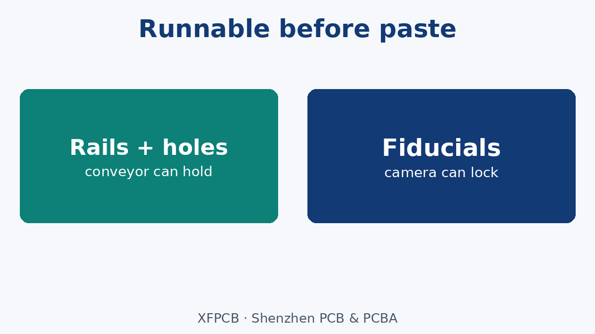
No process rails, no tooling holes, outline outside the conveyor window, or fiducials missing/wrong.
Fiducials need copper dots the camera can see: size in the assembler’s window, mask and legend clear of the copper, contrast keep-out, global plus local near fine-pitch when the house asks. Covered or undersized marks become placement alarms.
Rails and tooling holes belong on the panel note with the assembler’s pitch. An irregular singleton that will not sit on the belt needs a panel or a fixture—say which.
Bucket 2: Paste and joint physics
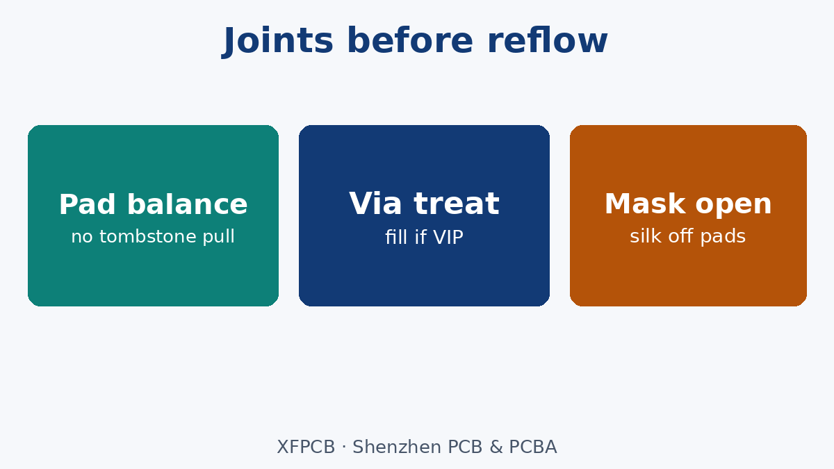
Pad geometry. Asymmetric pads and library footprints that ignore the vendor land pattern drive skew and tombstoning. Surface tension during reflow is not optional.
Via-in-pad. An open via under a pad drinks solder. If VIP is required, call filled/capped (or the fab’s named treatment) on the stack/fab note—silence is wicking.
Thermal imbalance. One termination tied into a huge pour while the other is a lonely pad heats unevenly; small chips tombstone. Thermal relief or balanced copper fixes the drawing, not the oven recipe alone.
Fine-pitch pad width/length. Pads too wide invite bridges; heels too short weaken joints. Use validated patterns, not stretched copper for routing convenience.
Mask and silk on pads. Mask encroachment and legend ink on solderable copper cause non-wet and intermittents. Keep openings and silk clear of the land.
Bucket 3: Inspection, rework and panel stress
Traces between fine-pitch pads that hide fillets from AOI, SMD spacing too tight for a nozzle, ICT pads missing or tented, and V-score/tabs that bend the board next to BGAs are yield after the first pass—rework and scrap. DFT pad rules are a sibling post; here the point is: if you will blame assembly for coverage, give the probe a land.
Panelization and copper balance affect warpage. Heavy clustering on one side without support is a mechanical EQ waiting to happen.
Wave and mixed technology, briefly
If THT parts see wave or selective solder, design for flow direction and solder thieves where the assembler uses them. A pure SMT drawing that later grows connectors without a wave note inherits bridging risk. Name the solder process on the assembly drawing when THT is in scope.
How this differs from CAM EQ theater
Factory DFM review will still raise EQs when files disagree or when you buy a harder class than the drawing implies. Fixing the buckets above reduces those EQs; it does not delete the review. Our PCB SMT Stencil path assumes pads and vias were already manufacturable. Our Manufacturing Files package is where panel, fiducial and VIP notes must appear.
What we are not claiming
No universal rail width or fiducial diameter as XFPCB law, no invented tombstone percentages, no claim that filled VIP is free, and no rewrite of the EQ-loop or “DRC vs CAM cost” posts. Lock rails, fiducials, pad balance, via treatment and mask opens on the drawing. Then SMT yield has a chance that process tuning can finish.