
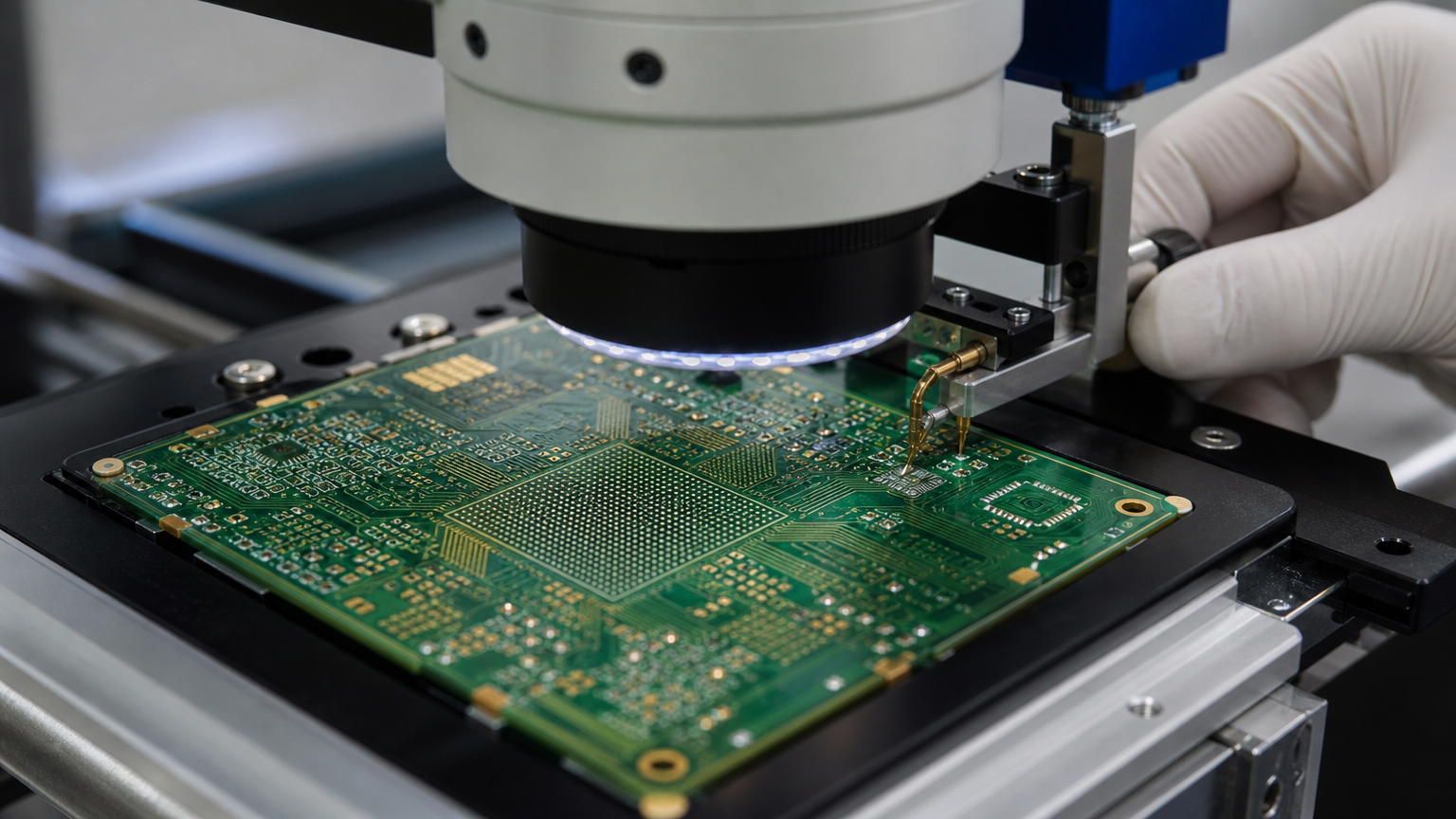
Inner-row balls on a 0.5 mm pitch BGA do not care how elegant your schematic hierarchy looks. Escape routing (fanout) - the short path from each pad to a via or channel - decides layer count, whether HDI appears, and whether the board is fabricable at the quoted price.
Routing globally before locking fanout is how teams discover mid-layout that they need via-in-pad, extra signal layers, or a pitch-driven stackup change. Treat the BGA as the floorplan center of gravity; place DDR, clocks, and PMICs to shorten critical escapes rather than painting yourself into a corner.
For package family context see the BGA and CSP packages guide. This article stays on multilayer breakout and DFM.
Pitch drives technology
Coarse pitches often allow dog-bone necks to through-hole vias between pads. As pitch shrinks, channels disappear and via-in-pad with filled/plated vias becomes the practical path. Thinner dielectrics, higher layer counts, and 1+N+1 or 2+N+2 HDI sequences follow when microvias must climb out of the pin field.
Estimate signal versus power/ground ball counts early. Power and ground can drop to planes; signal balls consume routing resources layer by layer. If inner rings cannot escape, add layers or change via technology before artwork is romanticized.
Breakout order and styles
Escape outside-in: clear the outer rings first so channels remain for deeper balls. Dog-bone fanout suits moderate pitch and cost-sensitive through-hole processes. Via-in-pad maximizes density when space between pads vanishes - budget fill, planarization, and solder-wicking controls with the fab.
Mixed breakout styles under one package increase manufacturing risk; keep the pattern consistent unless there is a documented reason.
Pads, mask, and via clearance
NSMD pads are common for BGA reliability and routing flexibility; confirm with the package and assembly house. Solder-mask bridges between fine pads are fragile - verify the manufacturer's minimum bridge capability before freezing pad diameter.
Keep via annular rings adequately clear of pad edges when dog-bones are used so mask and etch tolerances do not create shorts. Via-in-pad fill quality is an assembly yield item, not only a fab checkbox.
Stackup and SI while escaping
Every high-speed escape wants a continuous reference. Avoid launching pairs across plane splits. Limit layer transitions on multi-gigabit nets; each via is a discontinuity and potential stub. Orthogonal routing on adjacent signal layers reduces broadside coupling once you leave the pin field.
Back-drill or microvia strategies may be required when stub length threatens the channel - especially on thick boards.
Placement and mechanical keep-outs
Central BGA placement often balances routing and reflow symmetry. Multi-BGA systems need reserved channels between packages. Keep large BGAs a healthy distance from board edges where thermal gradients and handling stress peak during assembly.
Pre-tape-out checks
Fanout defined before global route, outer rings cleared first, reference continuity under high-speed nets, NSMD/mask rules confirmed, via-to-pad clearances met, layer-transition budget for critical nets agreed with SI, and fab capability (line/space, drill, VIP fill, HDI sequence) confirmed in writing.
Related process pages: HDI PCB and impedance control PCB. Send BGA pitch, stackup, and fanout notes with Gerbers via how to place an order.