Whether a via stub is long enough to hurt a channel is an electrical question: rise time, stub length, the dielectric, the rest of the loss budget. This article starts after that decision is already made. The stub has to come out. What the fabrication drawing has to say, and what a depth written in millimetres gets wrong, is a factory question.
What the drill is actually removing
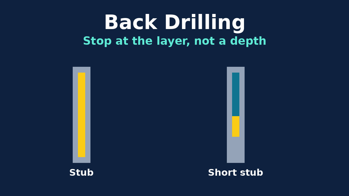
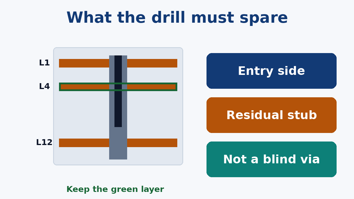
A plated through-hole is a barrel from one surface to the other. If the signal only uses the barrel down to an inner layer, the rest of that barrel is a stub. Back drilling comes back, after plating, with a larger tool from the unused side and cuts the plated wall away. The cut section is not plated again. It does not become a blind via. The connection that remains is still the original through-hole, shortened.
That is a different build from a blind or buried via, which never plates the unused length in the first place. Those vias are the structure an HDI PCB is planned around, including the extra lamination, rather than a drill added after the board is already plated. Back drilling keeps a conventional through-hole stack and adds a controlled-depth operation. It does not remove the need for the original drill, the plate, or the capture pad on the layer you still use.
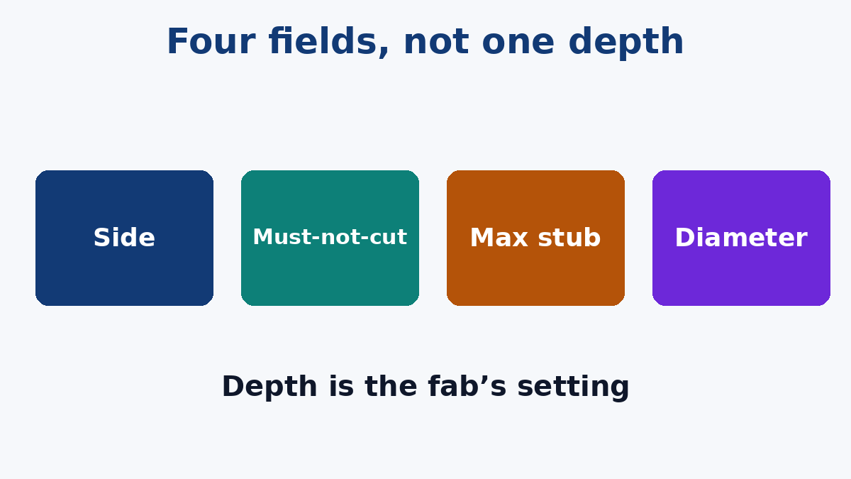
A stub can sit on the bottom, on the top, or on both if the only connection is in the middle of the board. Each direction is its own program: its own side, its own must-not-cut layer, its own depth. "Backdrill the high-speed vias" does not say which of those it is.
Why a depth in millimetres is the wrong note
Layer positions on a pressed board are not the positions in the CAD stackup. Prepreg compresses, cores have a thickness tolerance, and a panel is not perfectly flat. A target depth is a machine setting the fabricator calculates from the pressed construction, the side of entry, and the stub you are willing to leave. It is not a number the designer should freeze before lamination.
The number that belongs to the circuit is the maximum residual stub: the plated barrel still left between the last layer that must stay connected and the end of the copper the drill did not reach. It is measured from that layer, not from the board surface. The number that belongs to the process is how close the drill can come to that layer without cutting it, given depth tolerance and stackup variation.
Those two have to fit in the dielectric that is actually between the last connected layer and the next one down. As an illustration, a circuit that can live with 0.25 mm of stub and a process that wants 0.15 mm of clearance above the capture pad needs both of those inside the same gap. If the gap is thinner than that, the note is asking for a stub the board cannot physically provide, or for a drill that stops inside the pad. Neither is a depth the machine can "just hold." The fix is a stackup change, a looser stub allowance, or a via that was never a through-hole. It is not a tighter number on the same drawing.
A zero-stub callout is the version of this that opens nets. The drill has to stop before the capture pad and the barrel-to-pad junction. Some plated length will remain. If the circuit truly cannot stand that remainder, back drilling is the wrong structure.
Diameter is a third dimension, not a footnote
Three diameters get confused:
- Finished hole, after plating.
- Primary drill, larger than the finished hole by enough to leave room for the plated wall.
- Backdrill, which has to be larger than the primary drill, or it will not cut the whole barrel. A tool that is only a little bigger than the finished hole can leave a sleeve of copper in the hole. That sleeve is still a stub.
How much larger depends on plating thickness, drill wander and the shop's registration. State the basis so CAM does not have to guess it: oversize on the diameter relative to the primary drill, not a radial number written as if it were a diameter. The two conventions differ by a factor of two, and mixing them is how a drill is either timid or reckless.
Clearance to traces and planes is taken from the backdrill, not from the finished hole. The bigger tool, plus its positional tolerance, is what can nick a track or break an inner annular ring that looked fine against the via pad. If the backdrill also removes the unused pad on the layers it passes, say so. If those pads have to stay, the drill must miss them, which usually means the drill is too big for the note you wrote.
Vias that should not be on the list
Back drilling walks a tool through every layer from the surface to the stop. Anything that still needs copper on that path cannot be in the program.
- A through-hole that connects several inner layers, not just one, will lose the connections the drill passes.
- A must-not-cut layer very close to the entry surface leaves almost no room for tolerance. The stub you remove is short, and the risk of hitting the pad is not.
- Press-fit connectors need a plated contact length. Drilling that zone away, or roughing it, is a retention and contact problem, not a signal-integrity improvement. Keep press-fit holes off the backdrill list unless the connector vendor's remaining barrel still meets the contact zone.
- A via used as a probe point from the side you intend to drill will not be there for the fixture.
- A pair of differential vias should be drilled with the same side, the same stub allowance and the same diameter. One via backdrilled and its partner left long is a skew you added on purpose.
What proves it, and what does not
Bare-board electrical test checks continuity and isolation against the netlist. A via with a long stub, a via with a short stub, and a via with a thin sleeve of leftover copper can all read as the same net. Continuity does not measure stub length.
The direct check is a microsection through a coupon or a sacrificed via in each backdrill program: residual stub, the must-not-cut pad still intact, no leftover sleeve, and the drill roughly on the hole. One section does not represent every program if you have top-side and bottom-side drills, or several must-not-cut layers. Ask for a section per program when the stub length is the reason you bought the process.
A TDR or a set of S-parameters can show that the transition behaved as the channel model expected. It will not show a pad that was grazed on a via you did not probe. Our Testing & Inspection page is the electrical and visual side of a build. Treat backdrill depth as an added inspection, written next to the drill note, not as something the standard continuity report already covers.
A note CAM can run
Group the vias. For each group, write:
- Entry side, top or bottom.
- The must-not-cut layer, by layer number in the stackup you are actually ordering.
- The maximum residual stub the circuit allows.
- The backdrill diameter, and whether the oversize is on the diameter relative to the primary drill.
- Whether unused pads on the drilled-away layers are removed.
- Which vias are excluded: press-fit, probe points, vias that still connect on the drill path.
- That target depth is calculated by the fab from the pressed stackup, and that a zero stub is not the aim.
If the only sentence in the file is "backdrill to 1.6 mm," send the stackup and the must-not-cut layer before the job is tooled. The depth can be computed. It should not be the requirement.