
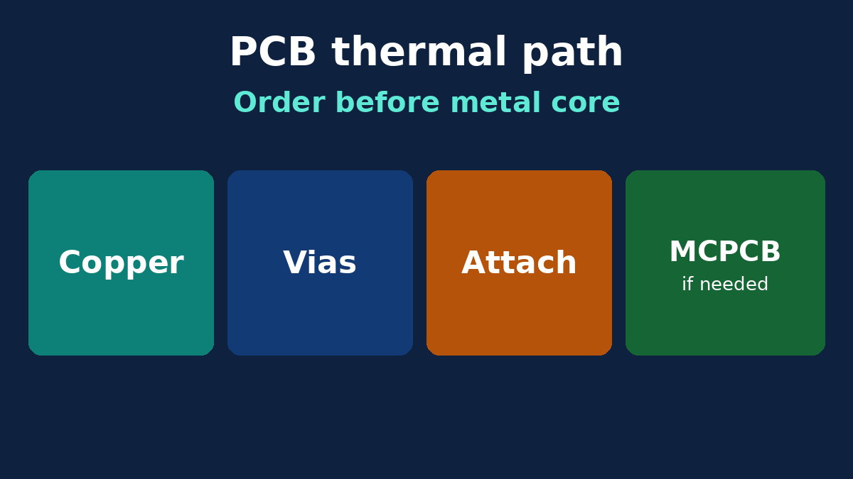
Heat leaves a board through a path. It does not leave because someone wrote “thermal management” on an RFQ. The useful question for a factory and for the layout owner is the same: where does the watt go next, and which of those steps are still open after the Gerbers freeze?
This post is that path order for overseas buyers and engineers. It keeps the industry facts that matter—copper spreading, thermal vias, mechanical attach, and when a metal core is actually the next step—and drops slogans, invented failure-rate percentages, and brand pitches. It is not a rewrite of how to debug an MCPCB stack that you have already chosen.
Start with the source and the sink
Name the heat sources on the schematic and the assembly drawing: which packages, roughly how many watts each under the operating case you care about, and whether that heat is continuous or pulsed. Name the sink: ambient air, a chassis wall, a cold plate, or a heat sink that bolts to a defined copper or metal face.
If either end is vague, every material upgrade is theatre. A thick copper pour that never reaches a sink is a warm plane. A metal-core board that never contacts a chassis is still a warm plate with a dielectric on top.
Path step 1: copper spreading on the same side
Before vias and before a special laminate, the first path is usually copper on the component side: pours under or beside the package, wide enough and continuous enough that the package’s thermal pad is not an island. The fab can etch that copper. It cannot invent a pour you never drew, and it cannot thicken a finished outer layer after the stack is pressed without a new construction.
Heavy copper helps when current and heat share the same geometry. It is a process and a cost change, not a sticker. Call out finished copper weight on the stack note if that is the lever you are buying. Our Heavy Copper PCB page is that construction family—not a substitute for a missing sink.
Path step 2: thermal vias to an inner or opposite plane
When the sink is on the other side of the board, vias move heat through the dielectric. A thermal via array under a pad is a layout feature: drill size, plating, whether vias are filled and capped for SMT, and keep-out from nets you must not short. Tenting a via under a thermal pad can trap air and block solder; open or filled-and-capped is a process decision you write, not a surprise on the line.
The factory drills and plates what you specify. It does not know that a via was “meant to be thermal” if the drawing never said so and the pad is a normal signal pad.
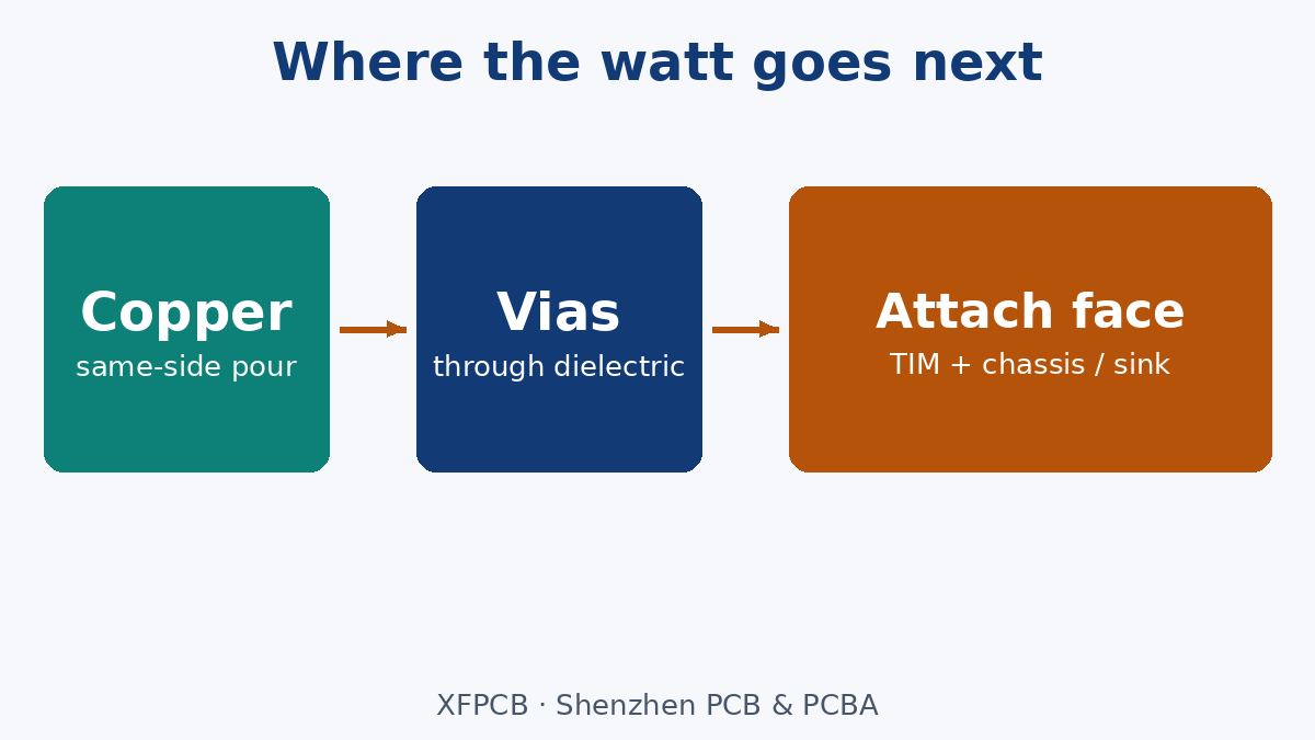
Path step 3: the attach face and the mechanical sink
Most of the watt still has to leave the board into metal or air. That is TIM thickness, flatness, screw torque, and whether the copper or the metal-core back is the contact face. Layout owns land pattern and keep-outs for the sink. The assembly drawing owns torque and TIM type if you care. The fab owns the flatness and finish of the face you named—not a heatsink you never designed.
Cold walls, thermal pads and spacing between hot parts belong here as mechanical and layout decisions. They are not a reason to skip steps 1 and 2.
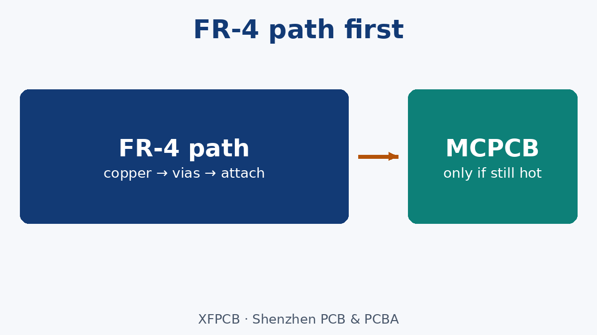
Path step 4: metal core only when the FR-4 path still fails
A metal-core or insulated-metal-substrate board replaces the glass-epoxy heat path with a thin dielectric over a metal plate. That is a different process traveler: usually fewer signal layers, holes that can short to the base if plated through carelessly, and a dielectric that is both insulation and thermal resistance. Our Metal Core PCB and Aluminum PCB pages describe that family. Use them when copper-plus-vias-plus-attach on FR-4 cannot meet the temperature rise you have measured or calculated—not because a generic article listed MCPCB under “thermal management.”
If you already know the job is metal-core, the bottleneck question moves inside that stack (dielectric, interface, chassis contact). That is a different post. This post stops at the decision to open that quote.
What the factory cannot fix after layout freezes
- Missing copper under a hot pad.
- No via array to the plane that faces the sink.
- A silhouette that leaves no flat attach area.
- A “6-layer aluminum” note with no stack: undefined job.
- Assuming electrical continuity test proves thermal performance. Continuity does not measure temperature rise.
What the factory can do inside a clear package: hold the copper weights and dielectric thicknesses on the stack, drill and plate the via array you drew, apply the finish on the attach face, and build MCPCB or aluminum IMS when that construction is the PO.
Applications without copying a pitch list
Automotive, LED and power-conversion boards often force this path early because watts are high and ambient is not office air. That does not mean every consumer board needs metal core, and it does not mean humidity or enclosure sealing are solved by changing the core. Sealing and thermal are separate drawings. Name both if both matter.
What we are not claiming
No percentage of industry failures “caused by heat,” no invented °C/W numbers, no claim that vias alone replace a sink, and no claim that XFPCB’s metal-core line is the default for every warm board. Thermal management on a PCB is the ordered path above. Lock copper, vias and attach before you spend the RFQ on a metal-core quote.