
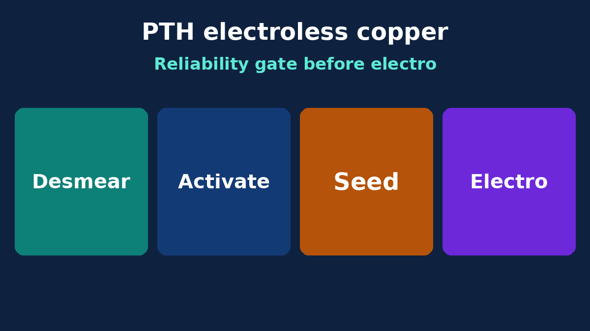
Plated-through reliability is decided before the panel sees electrolytic current. Electroless copper (chemical copper) lays a thin conductive seed on insulating hole walls so electrolytic copper can build the barrel. Chemistry encyclopedias list baths and half-reactions; buyers need the process gate and the failure modes that show up months later. Drill QA proves the wall is ready; this post is what happens next.
The gate in four stages (plus desmear)
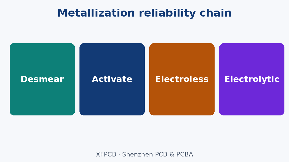
Treat the sequence as one reliability chain:
- Desmear / etch-back — remove resin smear from drill heat so glass and copper interfaces are clean enough to wet. Skip or under-desmear and palladium never sits where you need it.
- Clean / condition / micro-etch — strip oils and condition the dielectric so catalyst adsorbs; micro-etch refreshes copper surfaces for adhesion.
- Activation (often colloidal palladium) + acceleration — plant catalytic sites on the non-conductive wall; acceleration exposes the active cores.
- Electroless copper — autocatalytic reduction deposits a seed film (not the final barrel thickness).
- Electrolytic copper — builds structural PTH copper to the thickness your class requires.
Direct metallization (conductive polymer / carbon families) is an alternate hole-wall path some plants offer. If your drawing freezes “electroless copper,” do not silently accept a substitute without requalification.
What electroless is—and is not
Electroless copper exists so non-conductive walls become plateable. It is thin by design: a continuity and nucleation layer. Structural copper thickness, throwing power into high-AR holes, and surface copper balance are electrolytic (and pattern-plate) problems. Specifying only “1 oz PTH” without acknowledging seed + electro build confuses FAI thickness maps.
Formaldehyde-based and newer low-/formaldehyde-free systems both exist in industry. Buyers rarely pick the reducer; they pick coverage evidence and forbidden substitutions.
Failure modes buyers actually see later
| Later symptom | Often rooted in electroless / prep |
|---|---|
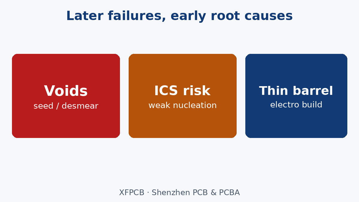
| Intermittent opens after thermal cycles | Thin or voided seed → weak electrolytic nucleation; interconnect separation (ICS) risk |
| Barrel crack / corner crack | Poor adhesion after smear left behind; stress risers at nail-headed inner Cu |
| “Plating voids” on microsection | Activation skips, plugged chips, or desmear not reaching resin |
| Inner-layer disconnect | Etch-back / smear balance wrong for that resin system |
| Patchy coverage in high-AR holes | Chemistry or time inadequate for aspect ratio—EQ AR limits, don’t hope |
Cross-sections after plating (and after stress when the class demands it) beat bath name-dropping. Ask where voids concentrate: entry, mid-barrel, or inner-layer junctions tell different root causes.
Desmear is not optional cosmetics
Drill heat smears resin over glass and copper. Electroless chemistry cannot reliably catalyze through that film. Desmear (chemical and/or plasma, per stack) is therefore part of the metallization gate, not a polishing step you can skip on “simple FR-4.” Resin systems differ; a recipe that worked on one mid-Tg laminate can leave smear on a filled or high-Tg stack. When FAI shows voiding at inner-layer junctions, ask for desmear evidence before blaming only the electroless bath.
What to freeze on the RFQ / fab note
- Hole metallization path: electroless copper + electrolytic (or a named alternate you already qualified).
- Any minimum electrolytic PTH copper and surface copper—seed is not a substitute for structural thickness.
- High-AR or blind/buried features that stress throwing power and desmear.
- FAI microsection expectations (locations, magnification class, void criteria you and the fab share).
- No silent bath or direct-metallization swap after qualification.
Our PCB Fabrication Process page places metallization in the flow. For copper weight capability context see Copper Thickness Capability. Evidence after build sits under Testing & Inspection.
What we are not claiming
No invented electroless thickness windows as XFPCB defaults, no palladium concentration recipes, no claim that one activator chemistry fits every resin, and no ITAR or aerospace plating certification pitch. Understand the gate—desmear → activate → electroless seed → electrolytic build—so EQ about voids and ICS lands on the right process owner.