
A stack-up that lives only in a designer’s head will be reinterpreted in CAM. Cores, prepregs, foils, and impedance layers are purchasing and process documents, not a pretty cross-section in a slide deck. This article owns how buyers and engineers lock a stack note that fabs will not casually rewrite: what must appear on the drawing, how book-build proposals get controlled, and which EQ loops appear when dielectric heights are “flexible.” It is not a tourist guide to “how many layers motherboards use,” and not a substitute for product pages on four-layer or multilayer boards—it is the document discipline that makes those builds repeatable.
Buyer decision frame: the stack note is part of the PO
Treat the stack-up PDF (or table in the fab drawing) as a controlled document with a revision, just like the BOM. It should answer:
- How many copper layers, and which are signal / plane / mixed?
- Which cores and prepregs (or slash-sheet / vendor PNs) build each dielectric?
- What foil starts on which layers, and what finished copper is required?
- Which layers are impedance references, with target ohms and trace geometry notes?
- What overall thickness and tolerance matter to the enclosure and connectors?
- Is the stack symmetric enough for warpage control—and who approves asymmetry?
If any of those are missing, CAM will fill gaps with plant defaults. Sometimes defaults are fine. Often they move impedance, thickness, or warpage. Lock the note before you chase price. For layer-count product context see Multilayer PCB Guide and 4-Layer PCB; this post is about freezing the sandwich those products build.
Cores, prepreg, and foil: name the building blocks
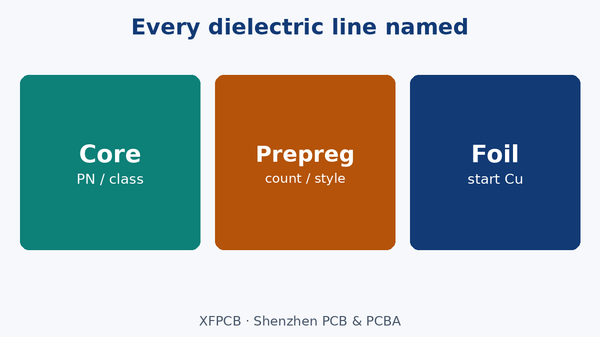
Cores are copper-clad laminates with defined dielectric thickness. Prepregs are the bonding sheets that flow in press. Foils add outer (or sometimes inner) copper. A stack is a sequence of these, not a vague “1.6 mm FR-4.” On the note:
- List each dielectric line with construction (e.g., core type/thickness or prepreg style/count).
- State copper weight start vs finished where plating adds copper.
- Mark which dielectrics are impedance-critical.
- Forbid silent swaps of prepreg count that change pressed height on those dielectrics.
Book-build (combining cores differently to hit the same total thickness) can be legitimate for materials availability—only with written EQ that restates dielectric heights on controlled layers. “Same overall mils” is not the same stack for SI.
Impedance layers: coupons must match the real nest
Impedance control fails when the coupon sits over a solid dielectric while the routed net sees a different pressed height or a swiss-cheese reference. On the stack document:
- Name target impedance classes and the reference plane layer(s).
- Tie coupon locations to the same dielectric construction as critical routes.
- Note glass style or material PN when skew/loss require it.
- Point to etch compensation expectations without leaving finished geometry undefined.
See Impedance Control PCB for capability framing—still put the numbers and references on your stack revision. Plants measure what you define; they do not infer your SERDES budget from a marketing layer count.
What must be on the fab drawing / stack PDF
Minimum contents that stop reinterpretation:
- Revision and part number.
- Layer table: copper layer names, types, foil/start copper, finished copper where specified.
- Dielectric table: material identity, construction, nominal pressed thickness intent for critical layers.
- Overall thickness and tolerance if mechanical fit matters.
- Impedance table: ohms, type (single/diff), layer, reference, coupon note.
- Via types overview if blind/buried/HDI change the stack (drill chart may live separately but must agree).
- Symmetry / copper balance notes if warpage-sensitive.
- Surface finish and solder mask do not replace dielectric identity—but list them so the traveler is one pack.
- “No substitution without written EQ” clause for impedance dielectrics.
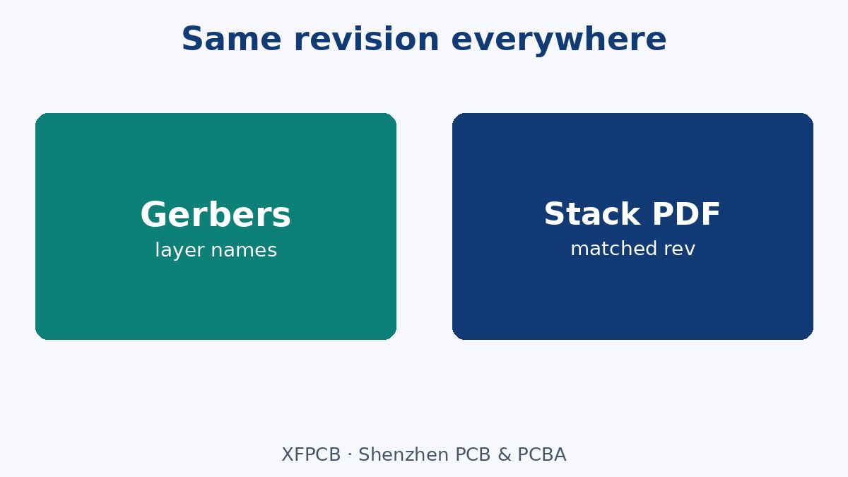
Attach datasheets for frozen PNs. Keep Gerber layer names consistent with the stack table—L2 in CAD must be L2 on the PDF.
Failure modes when the stack is soft
- Lot-to-lot impedance drift after a “equivalent” prepreg swap.
- Board too thick/thin for press-fit connectors or card guides.
- Warpage rejects after asymmetric copper or odd-layer temptations “fixed” in CAM.
- Blind via depth wrong because laser/mechanical stop layers disagreed with the note.
- EMI/SI issues when a plane layer was quietly turned into a mixed signal layer for routing convenience in CAM edits you never approved.
Fab can propose; you must approve. Soft stacks invite helpful CAM that breaks the product.
What fab can and cannot fix
Can: suggest manufacturable prepreg combinations; declare materials before press; hold for EQ when Gerbers disagree with the PDF; build to a frozen revision; add thieving when copper balance requires it without breaking keep-solid zones you named.
Cannot: preserve impedance if you allow free dielectric swaps; invent a stack from a 3D enclosure model alone; make an odd-layer fantasy cheap and flat; recover a pressed panel on the wrong book-build without scrap.
Odd layers, symmetry, and warpage
Even layer counts dominate production because foil pairing and mechanical balance are easier. Odd-layer requests often get converted or get expensive process exceptions. If you need asymmetry, document why and accept warpage risk controls (copper balance, bake, fixtures). Do not leave symmetry to tribal knowledge—put the expectation on the stack note.
Common EQ loop
- Designer sends a slide stack without PNs or pressed heights.
- Plant builds a convenient book-build.
- Coupons fail or connectors do not fit.
- Chat argument about whose stack was “//intent.”
- Second spin ships a revision-controlled PDF—should have been the RFQ.
Break the loop: no CAM start without a revisioned stack document aligned to Gerbers.
RFQ checklist for stack lock
- [ ] Stack PDF rev matches Gerber zip rev
- [ ] Material identity mode chosen (class / PN)
- [ ] Impedance table complete or explicitly N/A
- [ ] Overall thickness for mechanical fit called out
- [ ] HDI/via transitions agree with layer names
- [ ] Substitution rules written
- [ ] Contact for EQ named
Also freeze Manufacturing Files so ODB++/Gerber layer mapping cannot drift from the PDF.
How CAM typically “helps” soft stacks
When documentation is soft, CAM engineers do what plants do best: make a panel that presses flat, etches evenly, and uses stock cores. That help can include:
- Swapping prepreg styles to match warehouse stock.
- Changing core thickness and compensating with prepreg count.
- Adding copper thieving on planes you thought were solid.
- Renaming mixed layers to ease etch balance.
Each change can be reasonable in isolation and fatal for impedance or EMI in combination. The cure is not yelling at CAM—it is giving them a hard stack revision and a substitution clause. Invite proposals; require written approval before press.
Thickness tolerance and mechanical mates
Connectors, card edges, press-fits, and enclosures care about finished thickness. If your stack note only shows “about 1.6 mm,” plants will hit a nominal that may sit at the edge of your mate window after plating and mask. Call finished thickness and tolerance when mechanical fit is real. Remember mask and finish add to copper+dielectric—agree whether thickness is over copper, over mask, or as-received for the mating part. Put the metrology method in FAI when risk is high.
Cross-checking CAD layer stack managers
Exports from Altium, KiCad, or other tools are starting points, not contracts. Engineers often leave default dielectrics in the CAD stack manager that never matched the PDF sent to fab. Before RFQ, reconcile:
- CAD stack manager thicknesses vs PDF.
- Material names in CAD vs purchasable PNs.
- Layer order vs Gerber file names.
A mismatch here is one of the most common silent SI killers. Make reconciliation a release checklist item owned by the design authority.
Prototype stack vs production stack
Do not qualify SI on a four-layer prototype stack and then “cost-reduce” to a different dielectric height in production without re-running coupons and margin checks. Stack ECOs need the same rigor as schematic ECOs. Label prototype stacks clearly if they are temporary; do not let a temporary book-build become tribal production truth.
Cost traps without invented numbers
Under-documented stacks win the first quote and lose the second spin. Over-freezing every prepreg brand on a simple two-layer board wastes purchasing time. Changing stack mid-program without an ECO trail corrupts impedance history. Paying for impedance control without locking dielectric heights is paying for a certificate on a moving target. Document once; revise deliberately.
HDI and sequential laminate notes
When build-ups add laser dielectric layers, the stack document must show process sequence, not only final copper order. Which laminations happen when, which layers exist after each press, and where buried vias live—all belong in the note or an attached build flow. A flat list of eight copper layers can hide a two-press HDI flow that CAM must schedule. If your board is sequential, say so on the cover of the stack PDF.
Power and ground plane assignment is stack content
Labeling L2 “GND” and L3 “PWR” is stack content, not only layout preference. Mixed planes, split planes, and unused copper areas affect both EMI and press balance. If a plane is intentionally sparse, say whether thieving is allowed. If a plane must stay solid under an interface, put keep-solid language that CAM can see next to the stack—not only in a layout mail.
Panelization and stack notes
Panel borders, coupons, and thieving live on the same pressed sandwich. If impedance coupons are only on rails, ensure rail dielectrics match board dielectrics—or call out differences. If thieving is added only on panels, confirm it does not alter plane continuity assumptions inside the part. Stack lock includes how the panel expresses the stack, not only the singular board outline in CAD.
Communicating stack changes across sites
When design sits in one country and fab in another, stack ECOs need bilingual clarity: English stack PDF plus clear revision tags in the file name. Do not bury a dielectric change in a WeChat screenshot. Require the plant to reply with the material declaration (brand/PN) before CAM commit on every new revision. That reply is part of the quality record.
Coupling to return-path and plane rules
Stack documents assign which layers are ground and power; layout notes protect continuity on those planes. Keep both packs aligned. A stack that says L2 is solid GND while layout slots L2 under a connector is a product failure waiting for EMI lab time. Cross-link the documents in the release checklist so plane intent and dielectric intent ship together.
When quotes arrive with a plant-proposed stack different from your PDF, treat the proposal as a formal ECO candidate: compare dielectric heights on impedance layers line by line, update CAD if you accept, and re-issue the stack revision before first article. Accepting an oral “close enough” is how production drift begins. The cheapest time to reconcile stacks is at quote—not after stencils and fixtures exist.
Keep a single owner for stack revision control—usually the design authority—not purchasing alone and not the plant alone. Split ownership is how two “official” stacks appear for one part number.
Closing: make the sandwich purchasable
A stack-up earns its keep when purchasing can buy cores and prepregs, CAM can press them, and coupons measure the dielectrics you modeled. Lock cores, prepreg, foil, impedance references, thickness, and substitution rules on a revisioned document. XFPCB builds multilayer stacks from that freeze—not from a slide titled “typical 4-layer.” Send the document with the RFQ, and reinterpretation stops being the default.
If you take only one habit to the next RFQ: no Gerber release without a revision-matched stack PDF. That single gate prevents most of the helpful CAM reinterpretations that show up later as impedance and thickness failures. The sandwich is a document—manage it like one. Anything less invites CAM to finish the design for you.