
The motor-drive power stage cleared schematic review with margin: FET Rdson, bus capacitor ripple, and a spreadsheet that said 2 oz copper at the chosen width would keep Delta-T under 20 C. Prototype articles still failed the first load soak. IR thermography lit up MOSFET pads and a narrow neck into the DC bus pour, while the field team reported voltage sag at the connector under peak current that the schematic never showed. CAM had already warned that the 2 oz spacing was tighter than the shop's etch allowance and that the "thermal vias" under the FETs landed on soldermask with almost no copper on the opposite side. Nobody had lied in the current calc -- they had sized ounces in isolation and skipped the heat path and the fab rules that decide whether that copper survives etch and plating.
High-power boards for EV chargers, motor drives, inverters, and industrial PSUs fail the same way when buyers "just bump to 2 oz." Current, voltage, and total power are related but not interchangeable. Copper weight, width, layer location, and nearby planes belong in one sizing conversation. Heat has to leave the pad through pour, via array, plane, and sink -- not through a lonely via array. Materials and HV spacing sit on top of that stack. This guide is secondary original shop guidance for power engineers and buyers working with China fabs: how we read the intent, how IPC-2152 thinking replaces ounce folklore, and what belongs on the fab notes so heavy copper does not turn into a DFM fight after Gerbers land.
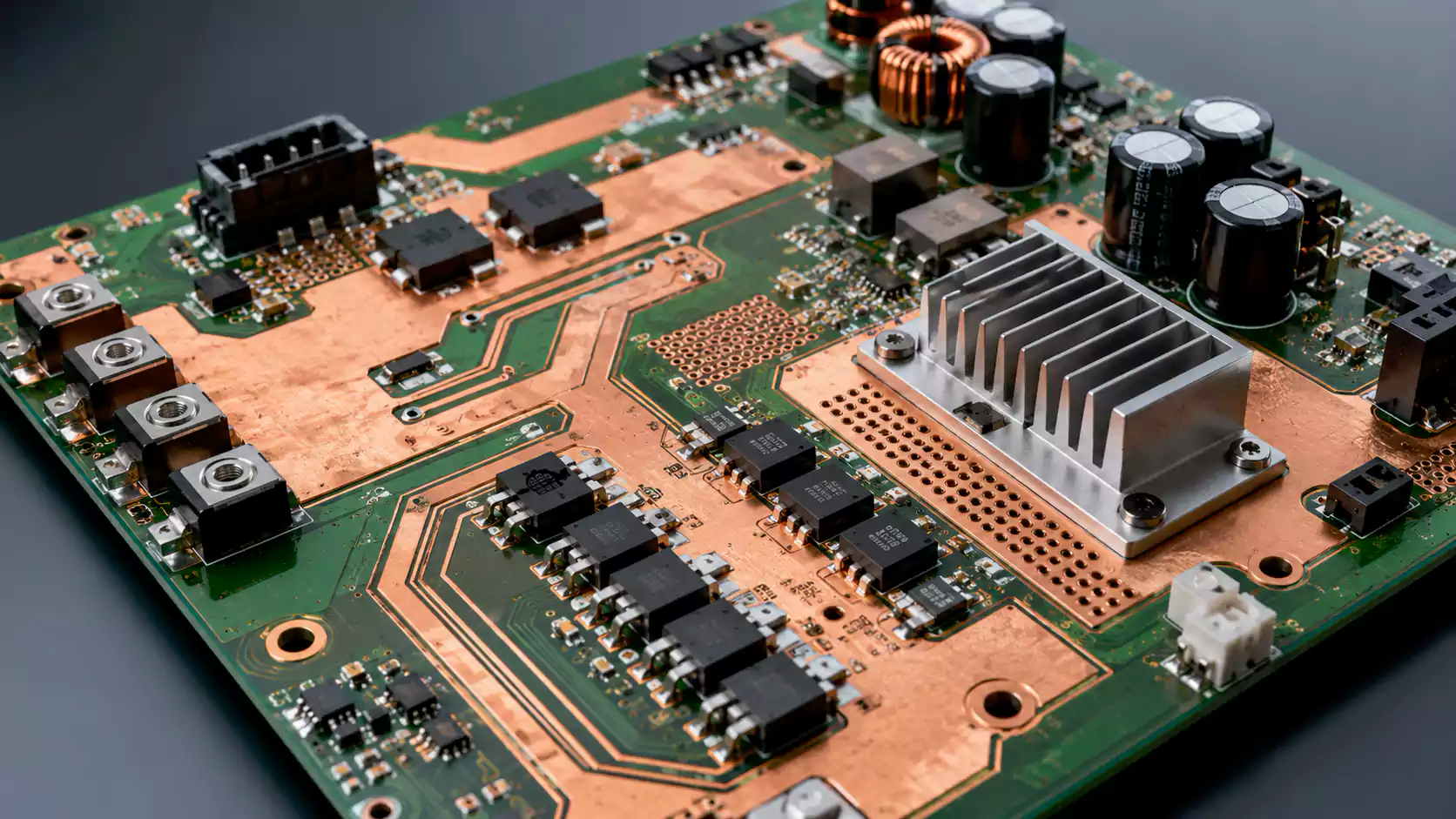
Separate the three intents before you thicken copper
High power, high current, and high voltage share vocabulary and often share a board outline. They do not share the same first constraint.
High power is about total energy moved and the heat and loss that come with it. The board may mix elevated current with elevated voltage. The design questions are copper loss, temperature rise, efficiency, and long-term reliability under continuous or pulsed load.
High current is about low resistance paths. Short, wide copper, thick foil or pours, power planes, and via arrays that actually carry amps dominate. Voltage drop and local heating on necks and via fields are the usual field failures.
High voltage is about insulation. Creepage, clearance, slotting, dielectric strength, and isolation between primary and secondary or between bus and control are the gate. Thick copper does not fix an undersized creepage path.
An EV charger or industrial inverter often needs all three on one traveler. Name which region is current-limited, which is voltage-limited, and which is thermally limited before you pick a blanket copper weight. That naming also tells CAM which notes matter: etch/space and via plating for heavy copper current paths, vs isolation drawings for HV zones.
Size conductors with IPC-2152 thinking, not ounces alone
"2 oz everywhere" is a quote shortcut, not a current rating. Conductor capacity is cross-section plus how heat leaves that copper. IPC-2152 is the modern reference for relating current, temperature rise, and conductor size. It improves on older IPC-2221 charts by folding in board thickness, dielectric behavior, and the heat-sinking effect of nearby planes and vias instead of treating a lonely external trace as the whole story.
Practical sizing still starts from the same physical levers:
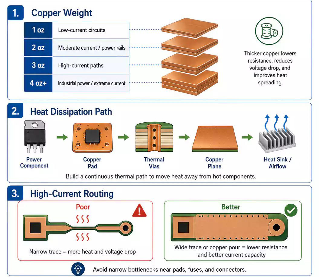
Copper weight (oz) sets thickness. One ounce is about 35 um; two ounces about 70 um. Heavier foil lowers resistance for a given width and adds thermal mass, but it does not cancel a long, narrow neck.
Trace or pour width sets the rest of the cross-section. Width and ounces move together. A narrow 3 oz finger can still run hotter than a wide 2 oz pour tied into a plane.
Layer location matters. External copper sheds heat better than buried inner copper. When high current must sit inside the stack, expect to widen the conductor or accept a higher rise than the external chart suggests. Older external-vs-internal derating habits remain useful as a conservative check even when you later refine with IPC-2152 charts or a thermal calculator.
Planes and pours change the answer. IPC-2152-aware practice treats adjacent copper as a heat sink. A trace that dumps into a solid pour or plane can run cooler than the same width sitting alone -- often enough to allow a more buildable geometry if the connection is solid, not a skinny thermal-relief spoke that starves both current and heat.
Temperature coefficient of copper resistance also bites under real load. As the conductor heats, resistance rises and voltage drop grows. Field sag that "should not exist" on a cold Ohms-law estimate often tracks that loop: hot copper, underestimated R, underestimated drop.
Work the numbers as a set: Imax, allowed Delta-T, copper weight by layer, width or pour geometry, external vs inner, and whether a plane is present. Then check voltage drop along the actual path length, including connectors and via transitions. If the spreadsheet only has "2 oz" and a single width from an old chart, you are still guessing.
Build a heat path that lands on copper
Thermography failures under MOSFETs, regulators, and power resistors usually mean a broken heat path, not a missing brand of laminate. A path that works in production looks like this in sequence:
Power device pad and solder joint to local copper pour on that layer. Then a dense thermal via array into inner or opposite copper that actually exists as a pour or plane -- not into empty soldermask. Then spreading on that plane or pour toward a chassis attach, heat sink footprint, metal-core base, or airflow region.
Via arrays are electrical and thermal bottlenecks when under-sized. Treat them as components: plating thickness, drill diameter, board thickness (aspect ratio), and count all set resistance and heat transfer. A handful of vias under a FET pad that never stitch into a large copper area on the far side move almost no heat. Dense arrays of modest plated holes that land on continuous copper on multiple layers do the work; filled and capped vias help when you need flat pads and better conduction under exposed thermal pads.
Direct copper connection under high-current pads usually beats aggressive thermal reliefs on those same pads. Reliefs help soldering of small passives to large planes; they hurt when the pad is the primary heat and current exit for a power FET. Prefer solid pour ties for the power path and reserve classic spoke reliefs for parts that would otherwise tombstone or cold-joint on a heat-sucking plane.
Validate under load. Simulation catches obvious hotspots early. IR on the first article under the same duty cycle the field will see catches the necks and via fields the schematic current calc never modeled.
Materials ladder without brochure language
Material choice follows heat density and voltage, not a catalog ranking.
Standard FR-4 remains fine for many moderate power and control mixes when copper and vias carry the thermal load and peak board temperature stays inside the laminate and solder joint budget. It is cheap and familiar; it is not a heat pipe.
High-Tg FR-4 is the usual step when continuous temperature, lead-free reflow exposure, or thermal cycling stress standard Tg. Industrial PSU, automotive-adjacent power control, and battery boards often land here before anyone needs metal core.
Metal-core (often aluminum MCPCB) earns its place when heat is concentrated and must move quickly into a sink or enclosure -- LED engines, compact converters, some power modules. The metal base changes mechanical and dielectric rules; it is not a drop-in substitute for a multilayer FR-4 power plane stack when you still need buried routing and dense control circuitry on the same outline.
Ceramic constructions (alumina, AlN-class, and related) sit at the high-temperature, high-reliability end where FR-4 and aluminum run out of margin. Cost and process differ enough that they should be a named requirement, not an afterthought on an FR-4 RFQ.
Hybrid approaches -- heavy copper outer layers on FR-4, selective copper coins, or metal-core power sections beside FR-4 control -- show up when one board must host both dense logic and a hot power island. Call the hybrid out in the stack table so CAM does not quote a single copper weight and a single dielectric as if the board were uniform.
Layout: short power loops and signal keep-out
Layout decides whether the copper you sized can be used. Keep high-current paths short and wide; every extra centimeter is resistance, drop, and heat. Switching loops around half-bridges and similar stages want minimum loop area so parasitic inductance does not turn into ringing, spike voltage, and EMI that then pollutes sense and control nets.
Separate power and signal geography on the floorplan. Gate drives, current sense, and feedback should not share a neck with the main power pour. Solid return planes under power stages help both EMI and voltage stability; broken returns force current around long loops. Place heat-generating parts where copper and airflow can work -- and where a sink can mount if the thermal budget needs it -- instead of trapping FETs against a connector wall with no pour escape.
Connectors and sense points belong on the electrical path you analyzed. Measuring "bus voltage" on a quiet pour while the load sees a resistive neck is how lab numbers disagree with field sag.
When high voltage shares the outline
If the same board carries hazardous bus voltage beside low-voltage control, creepage and clearance become first-class layout rules. Follow the isolation standard your product claims (and your safety lab will test), not a generic mil gap from a low-voltage design guide. Maintain spacing between primary and secondary, between high-voltage nodes and chassis-referenced copper, and across slots or barriers where the drawing calls for them.
Heavy copper complicates HV spacing because etch undercut and minimum space grow with copper weight. A clearance that looked fine at 1 oz can violate both fab capability and safety distance once you move to 3 oz or 4 oz without widening gaps. Call HV keep-outs on the fab drawing and keep soldermask and silkscreen from implying copper where isolation must stay open. Conformal coat or slotting may be part of the isolation story; say so in notes rather than assuming the fab will invent it.
Fab notes CAM needs for heavy copper
Heavy copper is a process change, not only a thicker foil callout. Etch undercut increases with copper weight, so minimum trace and space must open up. Typical shop guidance moves from fine-line 1 oz rules toward roughly 8 mil class features at 2 oz and wider still at 3 oz and 4 oz -- always confirm against the quoting fab's published capability rather than copying a generic chart into the drawing. Balanced copper across the panel reduces warp; large pours opposite empty regions invite bow.
Via aspect ratio should stay conservative for reliable plating -- many heavy-copper conversations aim near 6:1 or lower, with tighter ratios preferred on critical thermal or high-current vias. Call out plating thickness expectations, whether vias under power pads are filled and capped, and which layers carry 2 oz vs 3 oz vs signal-weight copper. Mixed copper weights on one stack are common; they must appear in the stackup table and in the traveler, not only in an email.
Write the RFQ in prose CAM can build from: copper weight per layer, min trace/space for those weights, via drill and plating notes, thermal via fill if required, impedance or HV spacing only where they apply, and the allowed temperature-rise or current intent for the power regions if you want DFM feedback against that intent. XFPCB quotes heavy-copper and high-power jobs from that package -- Gerbers, stack, and notes that admit ounces, width, planes, and heat path are one design -- not from a schematic current cell that assumed 2 oz would forgive every neck.
When the first article is sized that way, IR and field voltage usually stop surprising you. When they still do, the failure is localized and fixable: a pour that never reached the pad, a via array that never landed on copper, or a fab note that never matched the etch reality of the weight you ordered.