
The wearable RFQ called for a thinner stack, so the design team replaced a row of 0402 resistors with vacuum-deposited NiCr on the flex substrate and labeled the traveler "functional flex." First articles looked clean: fewer solder joints, less height under the elastomer, a single polyimide carrier for interconnect and trim. Bend qualification told a different story. After a few thousand hinge cycles the resistance values drifted outside the trim window, and one serpentine cracked where the film crossed the dynamic fold. The failure was not "flex is unreliable." It was functional film asked to live in the wrong mechanical class.
Buyers chasing thinner wearables, patch sensors, and medical skins often discover that limit at RFQ: embedded resistors and strain gauges earn their keep only when process, tolerance, and bend-zone placement are drawn like real fab constraints -- not as brochure synonyms for a bendable interconnect.
Functional flex is not just another interconnect FPC
A standard flex PCB answers two shop questions: how to route copper, and how to bend without cracking that copper. Coverlay, RA or ED foil, stiffeners, and bend radius dominate the traveler. A functional flex PCB keeps those jobs and adds a third: integrate electrical or sensing function into the substrate itself.
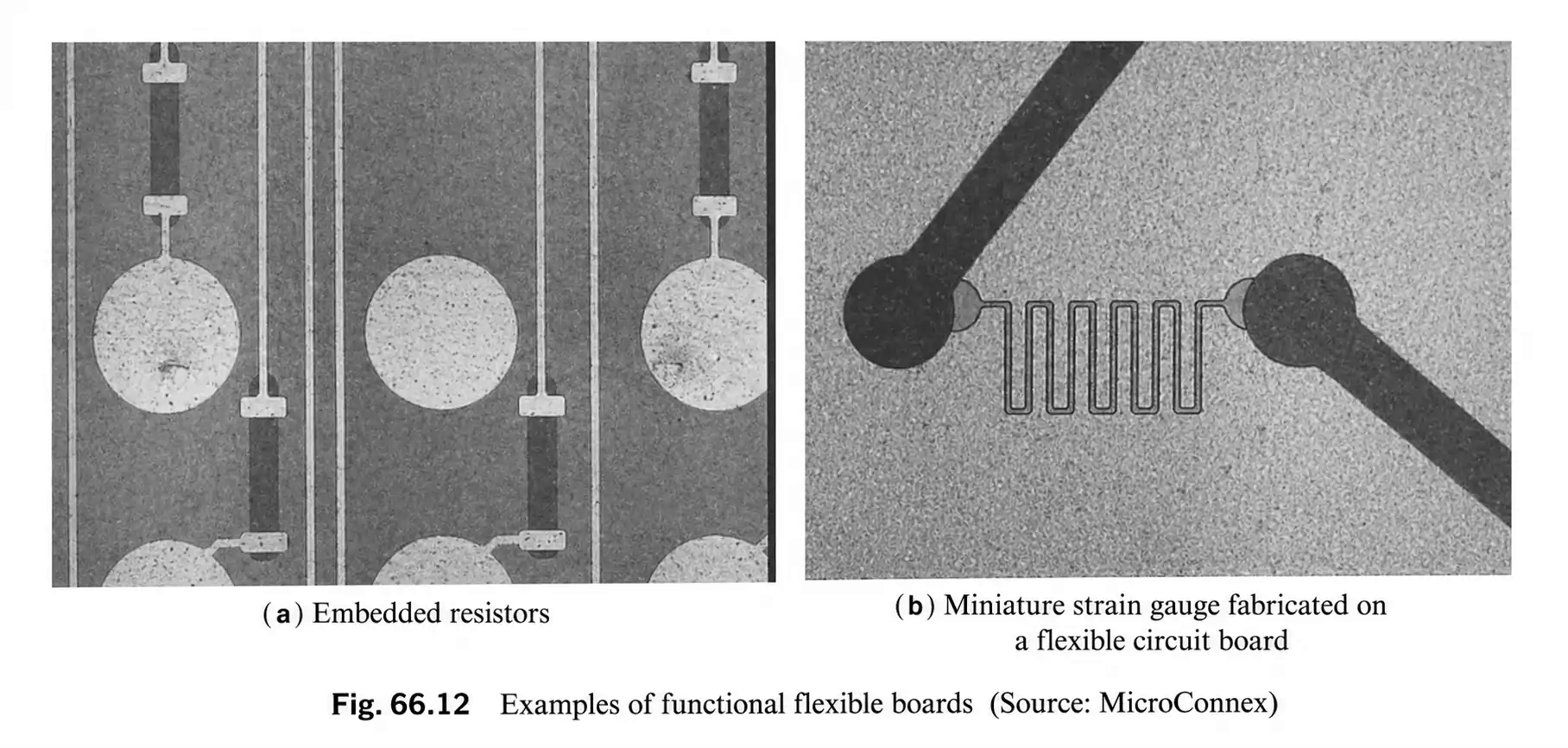
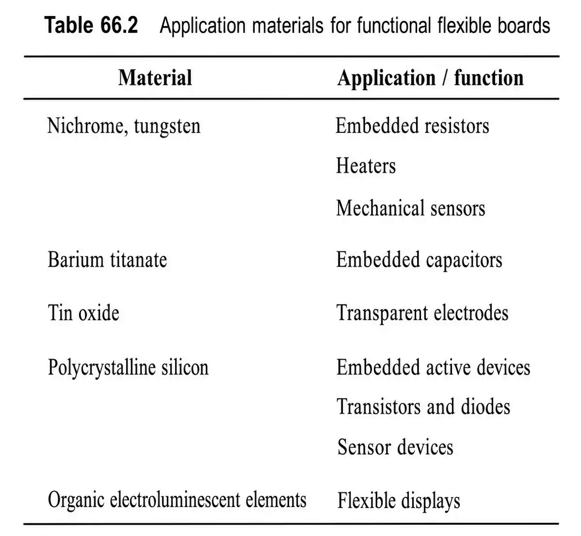
That usually means thin-film resistive alloys -- NiCr is the workhorse -- patterned as fixed resistors or as strain-sensitive gauges on polyimide. The board stops being only a cable or component carrier. It becomes a thin functional platform: interconnect plus trim, interconnect plus sensing, or both on the same outline.
The concept rhymes with embedded passives on multilayer rigid boards, but the mechanical duty of flex changes the rules. On rigid FR-4, film location is mostly about stack and heat. On flex, film location is also about whether that zone ever sees cyclic bend. Material datasheets for resistor foils say this bluntly: put embedded resistors in rigid portions; do not place them where dynamic flex will occur; flex-to-install is possible only with thorough testing because resistance can drift.
Why teams pay for functional flex at all
Space and assembly drive the cost. Wearables, catheter-adjacent electronics, and compact sensor modules often cannot spare the height or footprint of another row of discrete chip resistors. Every 0402 is a solder joint, a tombstone risk, and a local stiff spot under a soft enclosure. Forming the resistor in the film removes those joints from that zone and shortens the path between the sensing or trim element and the copper it serves.
Integration value shows up when the function must follow a curved or conforming surface. A strain gauge that is the flex -- not a glued-on sensor with its own leads -- tracks deformation of the same substrate that carries signal and ground. For products that already need FPC for packaging reasons, adding a functional layer can be cheaper than inventing a second mechanical assembly, provided the fab path and bend class are honest.
Functional flex is the wrong spend when the only goal is "make the cable bend." Ordinary interconnect FPC with RA copper and a correct radius still wins that RFQ. Buy the functional stack when embedded R or strain removes discrete parts, thins the module, or puts sensing where a discrete gauge cannot sit -- and budget the process control that thin films demand.
Two process paths shops actually quote
Vacuum-deposited NiCr. Nickel-chromium alloy is deposited as a thin resistive film on the flexible substrate, then patterned into resistor or gauge geometries. Sheet resistance is controlled by deposition and pattern aspect ratio (squares of film). The same family of films supports both fixed resistors and strain-sensing elements because NiCr's piezoresistive behavior and stable sheet ohms are well understood. Process control focuses on adhesion to polyimide, thickness uniformity, coverlay or overcoat protection, and how later lamination and coverlay press cycles shift the as-etched value.
Resistor-foil laminates (TCR / Pyralux-class). All-polyimide adhesiveless laminates that already carry a Ticer-style TCR thin-film resistor foil under copper are another production path. Public Pyralux APR-class notes describe NiCr (and related NiCrAlSi) foils with standardized sheet resistivity options commonly cited around 25, 50, and 100 ohms per square for NiCr, with broader TCR families extending toward 10 and 250 ohms per square depending on alloy. Material tolerance on the foil is often quoted near +/-5% before patterning and trim; finished resistor tolerance after etch depends on feature size, with wider geometries and laser trim used when tighter windows are required. Formation typically uses a multi-step etch that removes copper over the resistor body while leaving copper pads and leads. These laminates process much like familiar adhesiveless flex clads -- which is why fabs that already run AP-class material can extend into embedded R without inventing a new plant -- but the film still inherits the mechanical keep-out: rigid or stiffened zones first.
Neither path is "print a resistor and hope." Both need coverlay or dielectric protection over the film, controlled termination overlap onto copper, and an RFQ that states sheet ohms, target values, and allowed shift after lamination.
Embedded resistor use cases that justify the traveler
Embedded resistors earn the process when discrete parts fight the mechanical envelope. Typical wins:
Thin wearables and patches where 0402 height or solder under elastomer is unacceptable, and a handful of bias or termination resistors can live as film in a stiffened island.
Dense flex or rigid-flex modules that already push assembly real estate; moving terminations into the inner film frees copper for routing and reduces solder joints that fail under flex-adjacent strain.
RF and analog front-ends on thin carriers that want short, repeatable resistive paths without a forest of chip parts -- within the tolerance the film and trim can hold.
Compare honestly to discrete 0402. Chip resistors win on catalog tolerance, swap-out at ECO, and commodity cost when height is free. Embedded R wins on thickness, joint count, and co-location with the flex outline. Tolerance expectations must match the process: foil uniformity, etch geometry, and optional laser trim set the window -- not the +/-1% fantasy of a trimmed chip unless the fab path includes that trim step and you pay for it.
Embedded strain gauge use cases
Strain-gauge functional flex puts the sensing element in the same polyimide that bends or stretches under load. Applications include wearable force and posture sensing, soft robotics joints, industrial load patches, and medical skins where a glued discrete gauge would add stiffness or peel risk.
The gauge pattern (serpentine, grid) converts substrate strain into resistance change. That only works if the film is bonded and protected so that intended mechanical strain -- not crack, delamination, or uncontrolled creep -- dominates the resistance shift. Coverlay openings, adhesive choice, and local stiffening of bond pads matter as much as the alloy recipe.
Do not confuse "the product bends" with "the gauge belongs in the hinge." Many successful designs sense strain in a controlled flex-to-install or limited-motion zone while routing dynamic hinge copper separately with RA foil and proper radius. The sensing island is often stiffened or placed on a rigid-flex rigid finger so the gauge sees designed strain without seeing cyclic fatigue that opens the film.
Placement rule: keep functional films out of dynamic bend
Mechanical duty class is the gate that brochure language skips.
Static (flex-to-install) means the circuit is formed a few times at assembly and then sits still. Dynamic means repeated bend in use -- hinges, rolling wearables, continuous motion. Static work can use tighter radii and, in many shops, ED copper in the interconnect. Dynamic work wants RA copper, larger radius multiples of thickness, copper near the neutral axis, and no vias or pads in the bend. Those interconnect rules still apply on a functional flex job.
For resistive films the bar is higher. Industry resistor-foil guidance is explicit: apply embedded resistors in rigid portions of the PCB; do not place them in dynamic flex areas; flex-to-install placement is possible only after thorough testing because resistance values may change. In practice that means:
Keep NiCr resistor bodies and strain-gauge grids out of the dynamic hinge. Put them on rigid-flex rigid sections, on PI or FR-4 stiffened islands, or in static spans that never see cyclic fold.
Treat any film that must sit in a one-time form zone as a qualification item: measure resistance before and after forming, after humidity, and after the install bend profile you will actually use.
Separate sensing strain from fatigue strain. If the product needs both a hinge and a gauge, draw two zones. Stiffen or rigidize the sensing zone so intended load goes through the gauge pattern without cycling the film like a laptop hinge.
Interconnect copper in the dynamic zone still follows RA copper, neutral-axis, and radius discipline. Functional film does not get a free pass because the rest of the cable is "flex."
Misclassification is expensive either way. Putting TCR/NiCr film across a dynamic bend invites drift and cracks that look like process instability. Over-building a pure interconnect cable as "functional flex" burns material cost without buying a function the discrete BOM already solved.
What to put on the fab drawing and RFQ
Fabs quote what is drawn. For functional flex, say so in the stack and notes -- not only in an email subject line.
Name the process path: vacuum-deposited NiCr on polyimide, or resistor-foil laminate (APR/TCR-class or equivalent) with stated sheet resistivity (for example 25, 50, or 100 ohm/sq NiCr). List target resistor values, number of squares or geometry rules, and tolerance after etch and after coverlay/lamination. If laser trim is required, say so and mark trim access.
Map zones on the mechanical drawing: dynamic bend, static form, stiffened islands, rigid-flex rigid areas. Mark functional film keep-outs in dynamic regions. Show coverlay or overcoat that protects the film, termination overlap onto copper, and any stiffener that rigidizes sensing or resistor islands.
State mechanical class and cycle expectation for the interconnect hinge separately from the sensing or resistor islands. Call out RA versus ED copper by zone if the stack mixes them. Ask for resistance measurement points and any bend or form qualification the product will run so the fab's process window matches your acceptance.
XFPCB reviews functional-flex RFQs the same way we review EMI shields and impedance stacks: zone map first, material second, tolerance third. When embedded R or strain belongs on polyimide -- and stays out of the dynamic bend -- the thinner wearable or sensor stack is buildable. When the film is asked to be the hinge, the drawing needs a redesign before the traveler, not after bend qualification fails.