
Soldering tutorials usually describe how to make a joint: heat the pad and lead, feed the solder, let it cool. In production, nobody on the buyer's side makes a joint. What a buyer does decide—sometimes without realizing it—is which process each joint goes through, how many separate soldering steps the board needs, and what the joints must look like to be accepted. Those three decisions drive cost, yield, and reliability more than any iron temperature.
This article looks at production soldering from that buyer's position. It explains how an assembler routes each joint on a board to reflow, wave, selective, or hand soldering; what each route risks; what makes a board expensive to solder; and how to specify acceptance so that "good joint" means the same thing to you and your supplier. We write from XFPCB's assembly lines, where most boards combine at least two of these processes. For specific defects, see our articles on cold solder joints and related defect guides; this one is about process choice and acceptance.
Every joint has a route
When an assembler reviews your BOM and layout, one of the first engineering tasks is process routing: deciding how each part will be soldered.
- Surface-mount parts almost always go through stencil printing, placement, and reflow.
- Through-hole parts go through wave soldering, selective soldering, pin-in-paste reflow, or hand soldering.
- Heat-sensitive or late-fit parts (some connectors, displays, batteries, parts with plastic bodies not rated for reflow) are often hand-soldered or selectively soldered after reflow.
- Press-fit parts are not soldered at all but pressed after soldering.
The number of distinct routes on a board determines how many process steps it needs. A board with all SMT parts on one side has one soldering step. A board with SMT on both sides, a few through-hole connectors, and a hand-fitted part has four. Each additional step adds setup, handling, inspection, and risk. Design choices—part selection, side placement, footprint style—decide this routing long before the assembler sees it.
Reflow soldering: the default route
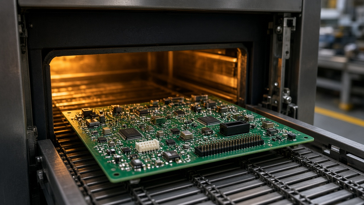
Reflow is the process for nearly all SMT parts. Solder paste is printed through a stencil, parts are placed, and the board passes through an oven with a controlled temperature profile.
What it depends on:
- Paste deposit. Stencil thickness and aperture design control paste volume, the most important variable for joint shape and defect rate.
- Profile. Preheat, soak, time above liquidus, peak temperature, and cooling rate must suit the paste, the components' ratings, and the board's thermal mass. Profiles are set by measuring actual board temperatures with thermocouples, not by oven settings alone.
- Component and board flatness. Warpage of large packages and of the board at reflow temperature causes opens and head-in-pillow defects on area arrays.
- Moisture-sensitive parts. Components with moisture sensitivity levels need controlled storage and floor life; violations cause package cracking or delamination.
Double-sided reflow. Boards with SMT on both sides go through reflow twice. The first side's parts must survive the second pass upside down. Heavy parts on the first side may need adhesive or be moved to the second side. Every part on the board sees two thermal cycles, which matters for laminate and component ratings.
What it risks: bridging, insufficient solder, tombstoning, voiding under thermal pads and area arrays, head-in-pillow, and opens from warpage. Most are controlled by stencil design and profile. See SMT PCB Assembly for how we set up the line.
Wave soldering: efficient for through-hole-heavy boards
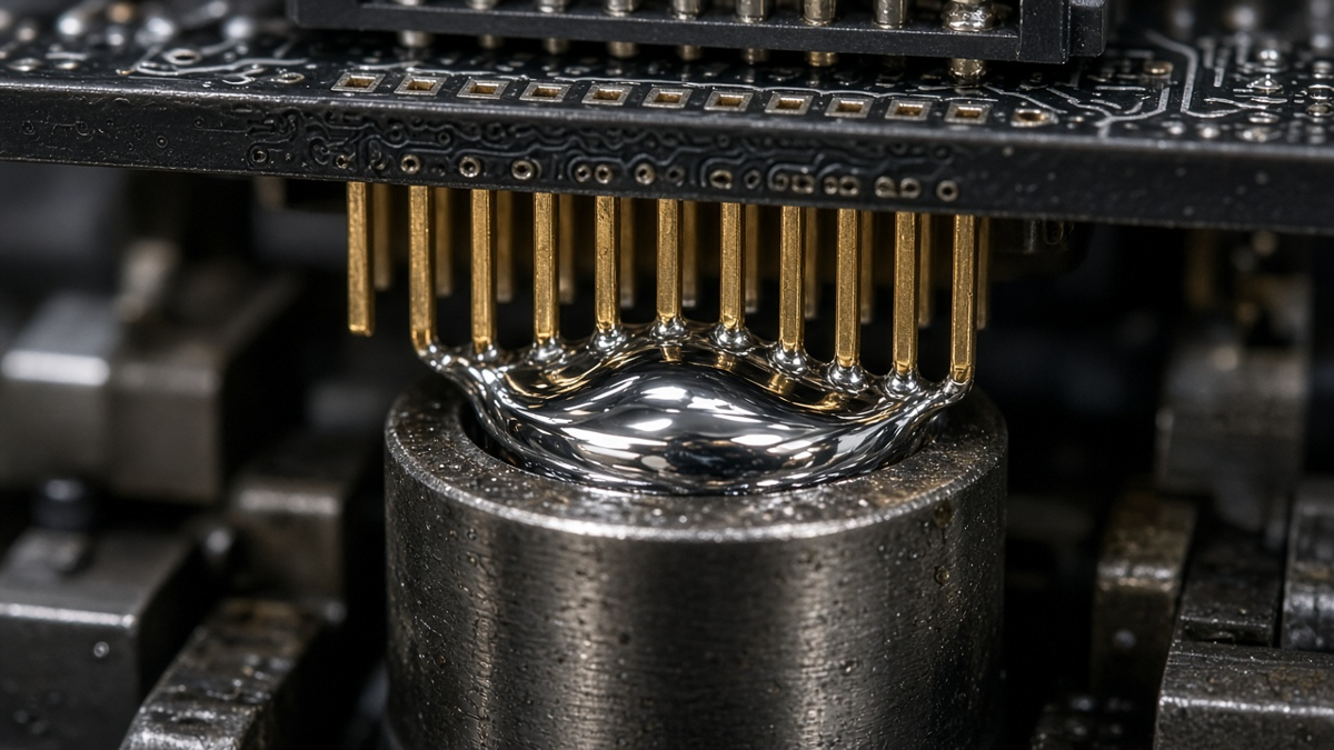
Wave soldering passes the whole bottom side of the board over a standing wave of molten solder after fluxing and preheating.
Where it fits: boards with many through-hole parts, where through-hole joints dominate, and where bottom-side SMT parts are absent, few, or wave-compatible.
What it depends on:
- Flux application and preheat so that the flux activates and the top side reaches a temperature that lets solder rise through the barrels.
- Contact time and wave dynamics set for the board's thermal mass.
- Board orientation relative to wave direction, which affects bridging on fine-pitch through-hole rows.
- Pallets that mask bottom-side SMT parts and support the board.
What it risks: bridging between closely spaced leads, insufficient hole fill on heavy copper, solder skips behind tall parts (shadowing), solder balls, and thermal stress on bottom-side SMT parts that do go through the wave. Bottom-side SMT parts that are glued and wave-soldered need footprints designed for it.
Selective soldering: targeted through-hole joints
Selective soldering uses a small nozzle—a mini-wave or fountain—to solder individual joints or groups of joints, programmed point by point.
Where it fits: mixed boards that are mostly SMT with a limited number of through-hole parts, boards with bottom-side SMT that cannot go through a wave, and joints that need individually tuned heat, such as connectors on heavy copper.
What it depends on:
- Clearance around through-hole joints for the nozzle; parts too close to the joint block access.
- Program for each joint or row: flux, preheat, dwell, drag speed.
- Thermal mass of the joint's copper connections.
What it risks: cycle time on boards with many joints, bridging if drag parameters are wrong, and insufficient fill on joints connected to large planes. It is slower per joint than wave but avoids masking pallets and exposes the rest of the board to less heat.
Pin-in-paste: through-hole joints in the reflow step
Pin-in-paste (intrusive reflow) prints paste over and into through-hole pads, inserts the through-hole part before reflow, and reflows it with the SMT parts.
Where it fits: boards with a few through-hole parts whose bodies are rated for reflow temperatures, when removing a separate wave or selective step is worth the extra engineering.
What it depends on: enough paste volume to fill the barrel and form fillets (often requiring overprinting or a step stencil), correct hole and pin sizes, part bodies rated for reflow, and parts that can be placed by machine or inserted before reflow without disturbing paste.
What it risks: insufficient barrel fill, paste pushed out by pin insertion, and part damage if the body is not reflow-rated.
Hand soldering: necessary, but controlled
Hand soldering remains part of most production boards: late-fit parts, heat-sensitive components, wires, and rework. In production, it must be a controlled process rather than an art.
Controls we expect and apply:
- Trained and certified operators, typically to IPC J-STD-001 for the class being built.
- Temperature-controlled stations with verified tip temperatures and tip selection for the joint.
- Defined solder alloy and flux, matching the rest of the assembly (do not mix leaded and lead-free).
- Work instructions per part, with photos of acceptable joints.
- Inspection of every hand joint, because hand joints vary more than machine joints.
What it risks: cold or insufficient joints on high-thermal-mass connections, pad lifting from excess heat or force, flux residue, and operator-to-operator variation. Boards that require many hand joints cost more and vary more; design and part choices that avoid them are worth considering.
What drives soldering cost
We do not publish price tables, but the cost drivers are consistent:
- Number of soldering steps. Each additional route adds setup, programming, handling, and inspection.
- Double-sided SMT versus single-sided.
- Through-hole count and access. Many through-hole joints favor wave; few favor selective; inaccessible joints force hand soldering.
- Pallets and fixtures for wave or for supporting thin boards.
- Special stencils such as step stencils for pin-in-paste or mixed paste volumes.
- Hand-fit parts, each adding labor and inspection.
- Inspection depth: X-ray for area arrays and bottom-terminated parts adds time per board.
- Thermal mass: heavy copper and large boards need slower profiles and more tuning.
Design choices that reduce cost without compromising function include grouping through-hole parts on one side, choosing reflow-rated parts where possible, keeping through-hole parts away from bottom-side SMT to allow wave or easier selective access, and avoiding parts that require hand soldering when an equivalent machine-solderable part exists.
Joint acceptance: say what "good" means
"Good joints" means nothing contractually. Acceptance should reference a recognized standard and a class.
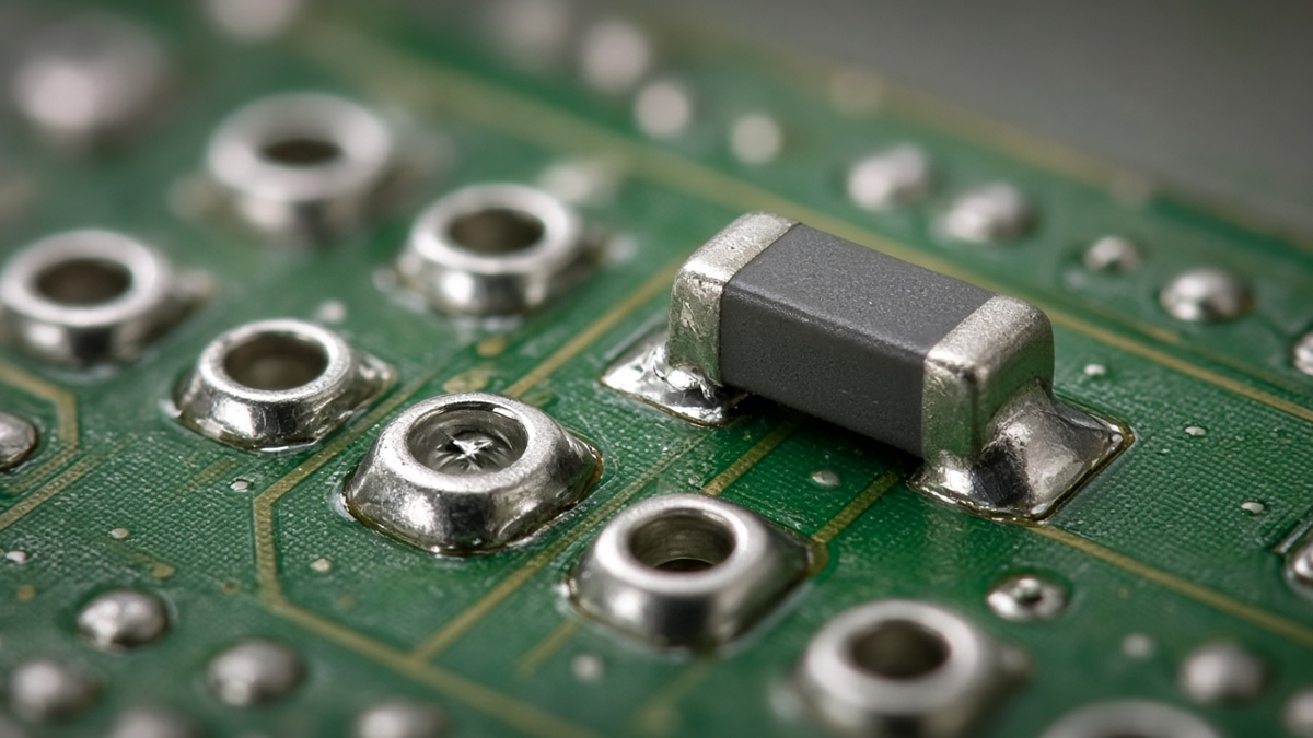
IPC-A-610 defines acceptability of electronic assemblies, including solder joint criteria for each component type—fillet heights, wetting, hole fill for through-hole, side overhang and end joint width for chip parts, and so on—for three product classes. IPC J-STD-001 defines the requirements for soldered assemblies, including process and materials controls. Most buyers specify IPC-A-610 at a given class; many also specify J-STD-001.
Choosing the class. Class 2 is common for dedicated service electronics where extended life is desired but uninterrupted service is not critical. Class 3 is for high-performance or harsh-environment products where downtime is not acceptable. Class 3 tightens criteria—for example on through-hole vertical fill and on certain fillet requirements—and usually increases inspection effort and cost. Ask for Class 3 where the product needs it, not as a default.
Mixed requirements. It is possible to specify Class 2 overall with Class 3 requirements for particular parts (for example power connectors or safety-critical joints). Write them by reference designator.
Hidden joints. Area arrays and bottom-terminated components cannot be inspected optically. Acceptance needs a method: X-Ray Inspection on a defined sample or on all boards, with voiding criteria agreed for thermal pads and balls where your design is sensitive.
Cleanliness. If you require cleaning or a specific cleanliness level, state it; no-clean flux residues are acceptable under many conditions but not all.
Cosmetic versus functional. IPC-A-610 distinguishes target, acceptable, process indicator, and defect conditions. Process indicators are not defects; they are signals for process improvement. Rejecting boards for process indicators creates disputes; tracking them creates improvement.
Process evidence a buyer can ask for
For critical builds, joint acceptance is supported by process evidence:
- Reflow profile records measured with thermocouples on a representative board, compared with paste and component limits.
- Wave or selective parameters for the program used.
- First-article inspection results for the first boards of a build.
- AOI and X-ray data with defect rates by type.
- Operator certification for hand soldering at the specified class.
- Rework records: which joints were reworked and how. IPC-7711/7721 describes rework and repair methods; many buyers limit the number of rework cycles per location.
You will not need all of this for every product. For first builds, new designs, and high-reliability products, ask for it.
Accepted is not the same as reliable
A joint that meets IPC-A-610 at final inspection has the right shape and wetting today. Whether it survives thermal cycling, vibration, or years of humidity depends on things inspection cannot see: intermetallic formation, voiding inside the joint, residual stress from warpage, and the match between component and board expansion. For products where long-term reliability matters, acceptance criteria should be paired with qualification evidence—thermal cycling or other environmental testing on representative assemblies—rather than relying on visual criteria alone. A change of soldering route, paste, or profile after qualification is a change that deserves review, even if the joints still look the same.
Lead-free versus leaded
Most commercial products are built lead-free to meet RoHS requirements; leaded processes remain in use under specific exemptions. The choice affects profile temperatures, component and laminate ratings, joint appearance (lead-free joints often look less glossy without being defective), and rework. Do not mix alloys on one assembly unless explicitly agreed. Our Lead-Free Assembly line runs lead-free profiles by default.
Buyer checklist for soldering requirements
- Workmanship standard and class (IPC-A-610 Class 2 or 3), with exceptions by reference designator.
- Process standard (J-STD-001) if required.
- Alloy: lead-free or leaded, and any specific paste or flux constraints.
- Cleaning requirement and cleanliness criteria.
- X-ray requirement and voiding criteria for hidden joints.
- Rework limits per location.
- Process evidence required for first article and production.
- Parts that must be hand-soldered or fitted after reflow, listed by designator.
- Any heat-sensitive parts with special limits.