
The internet likes a simple story: a modern CPU packs billions of transistors, so it must be able to amplify RF. Shop floor reality says no. Those transistors are digital switches sized for logic density and millivolts--not RF power devices you can bias, match, and heat-sink on a wireless board.
This article is for engineers and buyers who land on "can a CPU be an RF amplifier" and need a clear no, then practical RF PA PCB rules from a China fab that builds wireless and power-amplifier boards. It is not a joke post and not a "more transistors = more gain" myth.
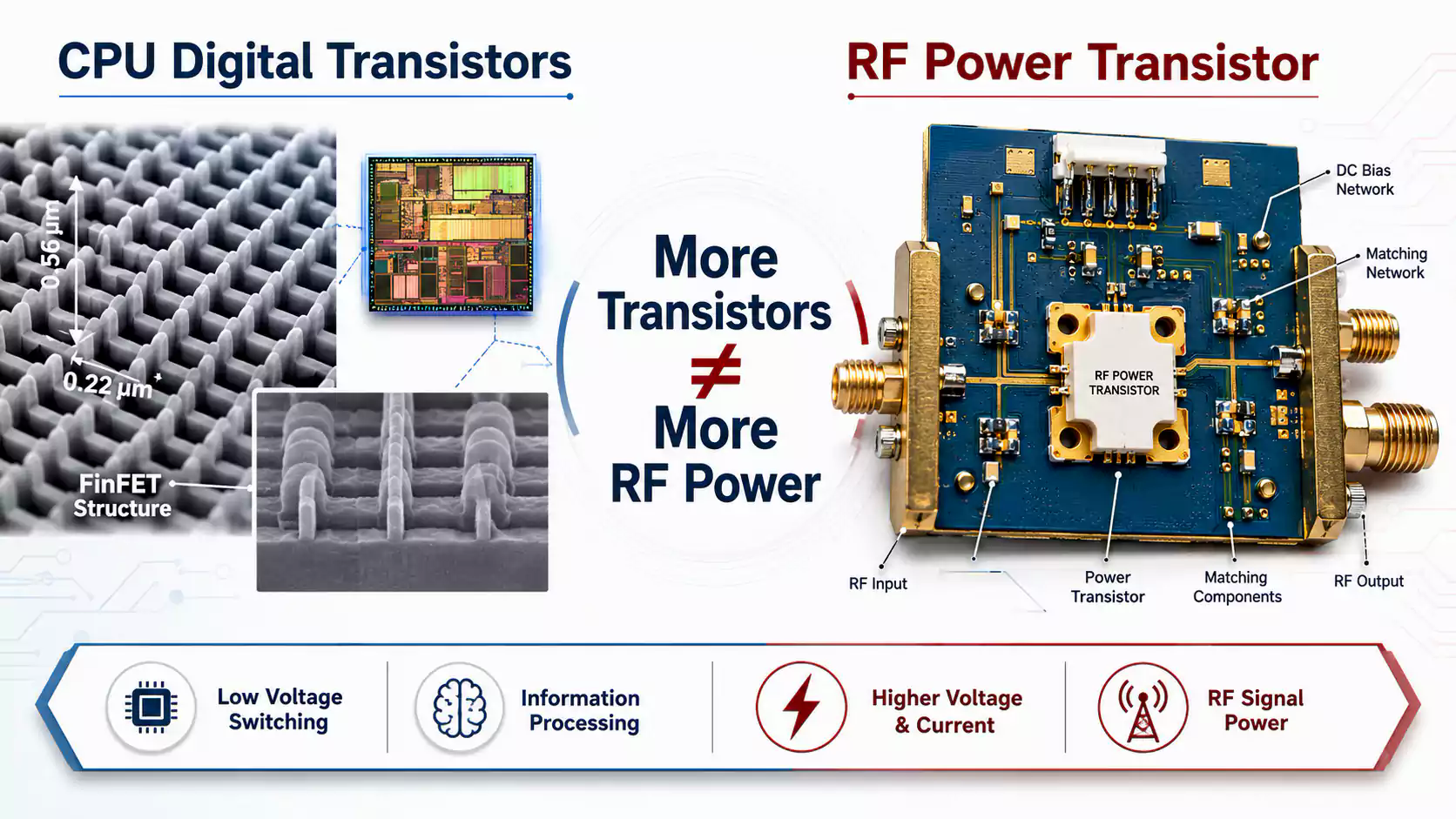
Billions of transistors is not RF gain
Transistor count measures how much digital logic fits on a die. It does not measure continuous-wave power gain, linearity, or PAE (power-added efficiency).
A CPU transistor is built to flip between logic 0 and 1 at very low voltage with tiny current per device. That is how you get dense cores, caches, and clocks without melting the package. An RF power transistor is built to take DC supply energy and put real RF watts (or milliwatts at microwave) into a matched load while staying stable and linear enough for the radio spec.
Same word--"transistor." Different job, different process, different package, different PCB around it.
CPU devices are digital switches you cannot treat as PA parts
Three shop facts kill the CPU-as-PA idea before layout even starts:
- Wrong physics -- Digital FETs are optimized for switching speed and leakage, not RF output power, breakdown voltage for the PA swing, or thermal paths sized for continuous dissipation.
- No usable RF ports -- You cannot wire-bond to an individual logic FET inside a CPU. Pins are digital I/O, memory interfaces, and power domains--not RFIN/RFOUT with defined reference planes.
- No amplifier chain around them -- A working PA needs bias, matching, decoupling, a clean RF ground, and heat removal. A processor package does not expose those building blocks for RF use.
So the answer is not "maybe with clever firmware." Firmware cannot turn a digital SoC into an RF power stage.
What an RF PA chain actually needs on the board
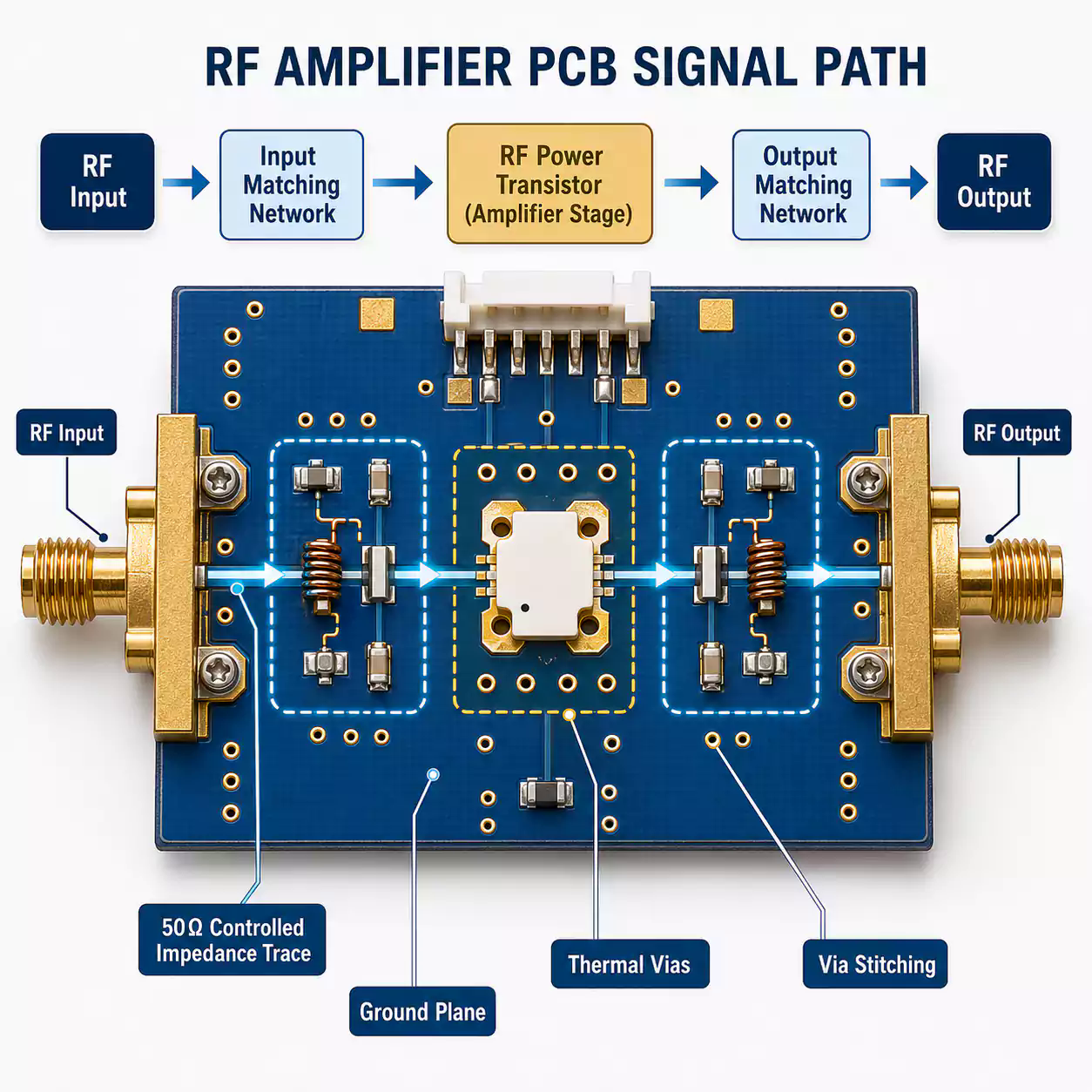
A practical RF power path is a chain, not a single chip drop-in:
- RF input connector or prior stage (filter, driver, switch)
- Input matching network close to the PA RF pin
- RF power transistor or PA module (GaAs, GaN, LDMOS, SiGe--per band and power)
- Bias / gate / drain supply with RF chokes and decoupling that do not open the RF loop
- Output matching into 50 ohm (or the system Zo) toward filter, coupler, or antenna
- Continuous RF ground reference under the chain
- Thermal path under the PA (paddle vias, copper pour, heat spreader or chassis)
Floorplan matters as much as the schematic. On a typical 4-layer PA module board, keep the switching regulator and noisy digital away from the RF corridor; run RF as a short, straight outer-layer path (often CPWG) with via fencing along the interconnect; put solid GND under the RF section on the next layer.
The PCB is part of the RF circuit
At RF, copper geometry is circuit, not just interconnect.
| Rule | Shop meaning | What fails if you ignore it |
|---|---|---|
| Controlled Zo (often 50 ohm) | Treat RF traces as transmission lines; width + dielectric height + copper + clearance must hit target | Reflections, lower delivered power, unstable PA |
| Match close to pins | Place matching L/C and shorts next to RFIN/RFOUT; do not stretch the match across the board | Detuned match, gain drop, possible oscillation |
| Continuous GND | Unbroken return under RF; no slot under the trace | Longer return, EMI, coupling, weird S11 |
| Short RF path | RF in -> match -> PA -> match -> RF out in a straight corridor | Extra parasitics, loss, radiation |
| Via discipline | Minimize RF layer hops; fence with ground vias; kill stubs | Inductance, resonance, leakage |
| Thermal | Copper area + thermal vias under the PA paddle; keep heat off the RF dielectric if possible | Gain droop, efficiency loss, early field failures |
| Keep switchers away | Floorplan buck converters and fast digital clocks off the RF region | Spurs, desense, failed EMC |
Altium-style PA module practice (4-layer, CPWG RF, via fencing, regulator kept clear of RF) matches what we see on real wireless RFQs: the stackup and floorplan are part of the amplifier, not decoration.
When FR-4 fails and low-loss material earns the cost
FR-4 (and mid-loss FR-4 family laminates) still work for many short RF paths at lower GHz when insertion loss budget is loose and interconnects are short. That is why some compact PA modules stay on low-Dk FR-4-class material when the RF run is only a few centimeters.
Step up when any of these show up on the traveler:
- Band and length where Df (dissipation factor) eats too much of the link budget
- Tight impedance tolerance on thin dielectrics where Dk drift hurts match
- Higher power where heat plus loss compounds
- Outer-layer RF that still needs smoother copper and stable Dk/Df across temperature
- Hybrid builds: RF outer on Rogers/Isola/Taconic-class HF material, digital inners on FR-4 where process allows
Material choice is a cost dial, not a brand trophy. Spec Dk/Df at the frequency that matters, copper profile if loss is critical, and which layers are HF versus digital. Do not pay for low-loss laminate on every layer of a mixed board when only the RF skins need it.
What CAM needs on an RF PA RFQ
Incomplete RF packages get treated like ordinary digital boards. CAM opens Gerbers, sees "FR-4, 1 oz, 4 layer," and has no reason to ask about Zo, via fencing, or which layers are actually RF.
A usable package names the stackup with materials and copper weights, puts an impedance table next to it (target Zo, tolerance, which nets, microstrip or CPWG or stripline), and states the band plus the PA part or at least the power class. Ground notes should say the RF corridor sits on continuous GND and whether a via fence pitch is required. Floorplan callouts that keep the switcher and fast digital off the RF zone save a later EMC fight. Under the PA, say how heat leaves the paddle--thermal vias, pour, coin, or chassis interface--and whether solder mask stays on the RF traces or comes off for loss. If you will TDR or VNA the board, mark coupon or SMA locations on the fab drawing. Assembly jobs add BOM and CPL the same way as any other wireless PCBA.
Send that package through support or how to place an order. XFPCB builds high-frequency and controlled-impedance boards for wireless and PA work when those notes sit on the drawing.
A CPU still cannot be the amplifier. Transistor count is not RF gain, and a processor package does not hand you RF ports, bias, matching, or a PA thermal path. Use dedicated RF power devices, keep the PCB part of the circuit, and spend laminate dollars where the band and length actually demand them.