
The ADC channel that looked perfect on the bench sketch hopped a few LSBs whenever the nearby SerDes lane burst traffic. The clock that passed timing simulation grew a skirt on the spectrum analyzer. EMI pre-scan put a peak right on a harmonic of the core switching edge. Layout had sprinkled 0.1 uF ceramics beside every power pin. The schematic was tidy. The loops were not.
Those failures read like signal-integrity bugs. On the shop floor they usually start as power-delivery geometry: the capacitor value was fine, but the pin-to-cap-to-via-to-return path was long enough that high-frequency current never saw a low-impedance reservoir. This article is secondary original placement language for engineers whose boards fail EMI, ADC, or clock work with "0.1 uF everywhere," written from a China fab DFM desk that sees Gerbers before the spectrum plot. Capacitance tables alone do not fix a large loop.
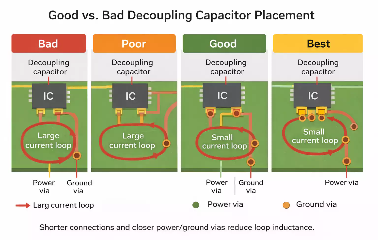
"Close" means loop inductance, not a tape-measure number
Shop talk says put the decap next to the pin. High-frequency PDN care says shrink the loop that carries the transient: IC power pin, capacitor body, ground or return, and the vias that stitch into planes. Physical millimeters matter only as they drive that loop area and series inductance.
A part that looks adjacent can still be electrically far. A narrow neck from the ball or pad, a dogleg around silk text, a ground via parked a package length away, or power and ground vias split across opposite sides of the footprint all inflate ESL even when the ceramic sits in the CAD "near" zone. Straight-line distance on the silkscreen layer is a weak proxy. The current path length and the enclosed area are the metrics that survive the first RF measurement.
When planes are weak or widely spaced, that loop language is unforgiving. When planes are tight and continuous, the planes themselves carry some of the fastest energy -- but the discrete capacitor still has to recharge them through a low-inductance entry. Either way, judge placement by pin-cap-via-return, not by how neat the 0.1 uF symbols look in the schematic grid.
Pin, capacitor, and via geometry that kills HF noise
Treat the local network as four connected pieces of copper, not a floating BOM line:
- Land the capacitor pad as near the power pin as the package escape allows.
- Connect pin to capacitor with the shortest, widest copper the land pattern permits -- no meander for "pretty" routing.
- Put the power via at the capacitor pad edge (or in the pad when VIP is in the traveler), not after a stub of routing.
- Pair a ground via immediately beside the power via so the return closes in a tight vertical pair instead of a sideways hunt across the board.
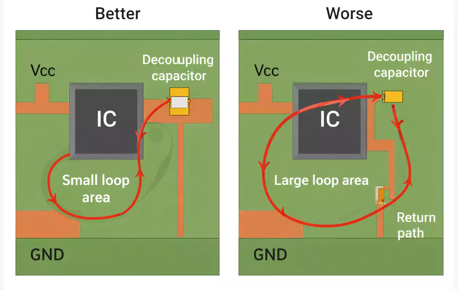
Via pairing is not decoration. Separated power and ground vias open a horizontal loop that shows up as inductance long before the ceramic's datasheet ESL does. Shared vias between neighboring caps look efficient in a dense field and then couple the loops; give each local HF cap its own power/ground via set when space allows. Routing a signal between the capacitor and the pin forces the transient current around an obstacle -- that copper belongs to the PDN loop, not to a convenience channel for an unrelated net.
Package size is part of the same geometry. Smaller bodies (0201, 0402) typically carry less mounting inductance than larger footprints of the same nominal value, which is why HF local caps favor small ceramics. Assembly yield, stencil aperture, and rework skill still gate how small you can go on a given line -- more on that in the fab notes below.
Multi-value networks without anti-resonance superstition
One 0.1 uF does not cover every decade the IC demands. Bulk parts (often tens of microfarads near the regulator or rail entry) handle slow load steps. Mid-value ceramics support intermediate edges. Small, low-ESL ceramics next to the pin answer the fastest di/dt. That tiering is shop language for frequency coverage, not a superstition that every decade needs a different magic number.
Anti-resonance between mismatched values is real in PDN plots, but the cure is not "never mix values." It is to place and connect each tier for the job it owns, keep HF caps in the tightest loops, and avoid dumping wildly different parts into one shared via farm where their inductive tails fight. Parallel same-value ceramics reduce effective ESL when mutual inductance stays low -- useful under BGAs and dense digital rails. Spreading identical small caps around a power domain usually beats one oversized can parked "somewhere nearby."
Start from the IC datasheet rail notes, then adjust for your measured or simulated target impedance. Datasheet defaults that assume a reference escape will not forgive a layout that doubled the loop. Value selection without placement discipline just moves the resonance while the EMI peak stays.
When plane spacing changes the placement game
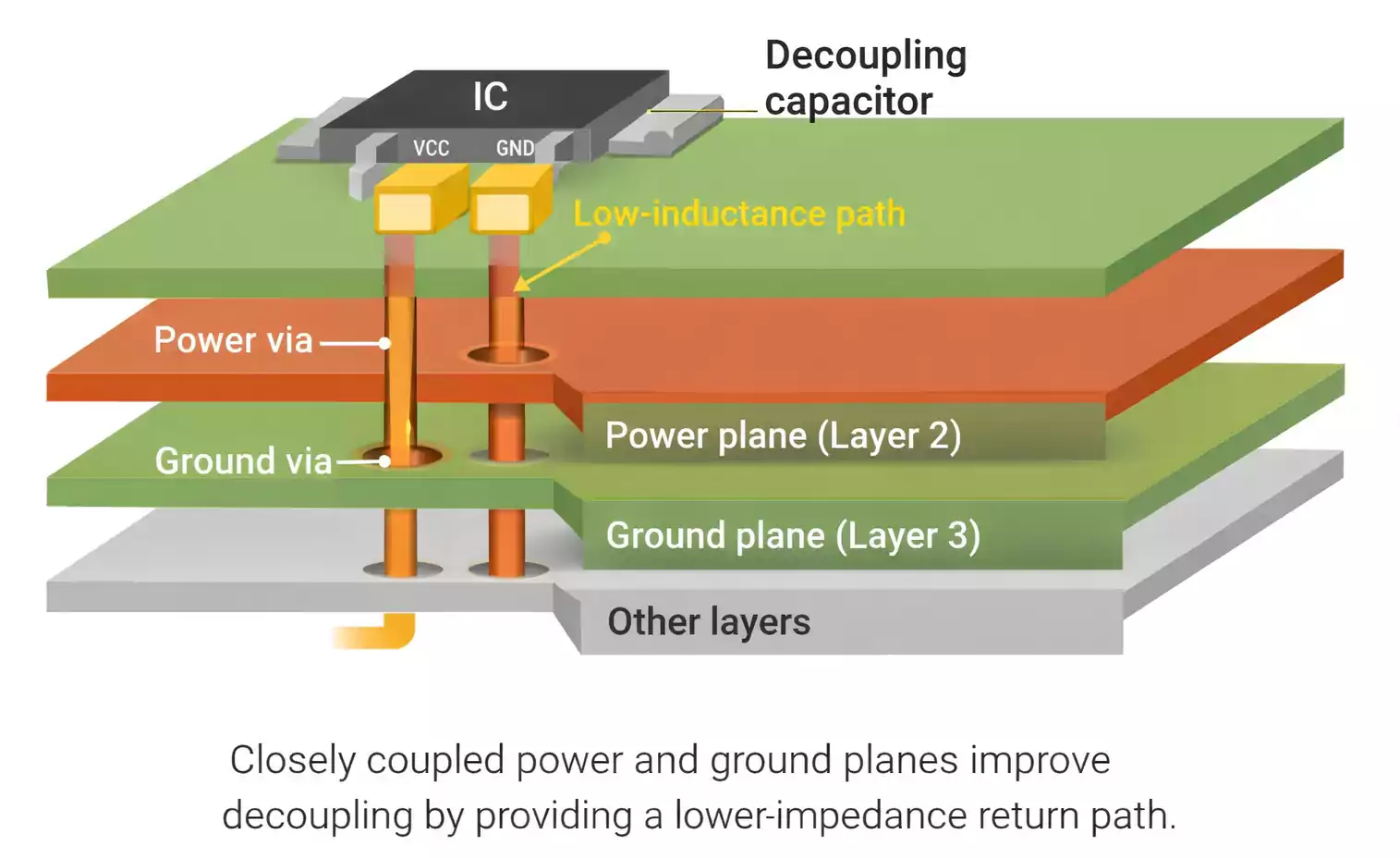
Boards without solid power/ground planes live or die on discrete loops. Every active device needs local ceramics with minimal area, plus bulk on each rail near the entry. There is no distributed plane capacitance to hide behind.
Closely spaced power and ground planes (on the order of a few mils / tenths of a millimeter in many multilayer builds) form useful interplane capacitance with very low series inductance. At the highest frequencies the planes can deliver energy faster than a distant ceramic. Local caps then sit in a "vicinity" role: close enough to recharge the planes on the timescale of the edge, not necessarily glued to every single ball if the plane entry is already low inductance. Horizontal clearance can relax a little; vertical connection quality -- short vias into those planes -- cannot.
Widely spaced planes (classic thick four-layer recipes with a large core between power and ground) contribute little high-frequency capacitance. Placement snaps back to same-side, pin-adjacent discipline. Opposite-side caps on ordinary QFN/QFP packages add via height that often hurts more than it helps. Pair opposite-polarity vias tightly near the pins and keep the capacitor on the IC side unless density forces another answer.
Plane splits under a decoupling loop erase the benefit either way. If the return has to detour around a gap, the loop grew whether or not the silkscreen said "0.1 uF nearby."
BGA underside versus QFN same-side
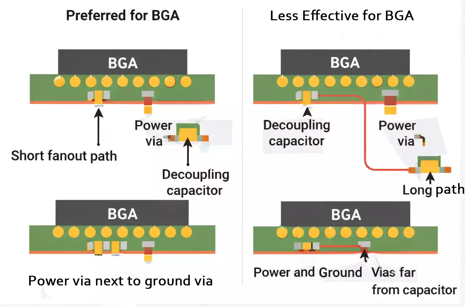
BGA ball maps eat surface real estate. Placing ceramics on the opposite side, under the package, on the power and ground vias that already serve the balls is often the shortest HF path available -- shorter than a same-side part parked several millimeters outside the shadow. Via-in-pad (filled, plated, planarized) tightens that path further when pitch and fab capability allow. Perimeter placement outside the BGA can still work when underside copper is full; keep fanout vias short and pair returns.
QFN, QFP, and similar leaded or land-grid packages usually win on the same side as the IC. Flipping a local HF cap to the back for cosmetic crowding adds via inductance that the package did not force you to take. Reserve backside local caps for BGA-class density problems or explicit HDI stack decisions, not as a default cleanup move.
Under either package, connect pin (or ball via) to capacitor first, then into the plane structure. Inserting a long trace between pad and via turns a good footprint into a series inductor with a ceramic hanging off the end.
Assembly notes fabs actually build
From the traveler side, high-frequency decoupling succeeds only when the geometry survives CAM and SMT. Call out via-in-pad early when underside BGA caps or dogbone-free escapes need filled and capped vias; VIP changes drill, fill, plate, and planarize steps and shows up in quote and lead time. Name the capacitor package mix (0201 versus 0402 versus 0603) so stencil design and placement nozzles match the density you drew -- a field of 0201 under a large BGA is a different process window than scattered 0603 along a QFN edge.
Ask for continuous reference under the rails you care about, and mark keep-outs that protect the pin-cap-via copper from unrelated routing. If microvias or stacked structures feed the local PDN, say so beside the stackup table rather than hoping CAM infers intent from a crowded Gerber. XFPCB can confirm whether the VIP, package size, and plane spacing in the RFQ are buildable before the layout team locks a loop that manufacturing cannot reproduce.
Placement language on the fab drawing should sound like the lab failure you are trying to prevent: short pin-cap-via-return, paired vias, tiers that cover the edge rates you actually switch, and package sizes the line can place. Nominal 0.1 uF stamps without that geometry are how ADC hops and EMI peaks survive another spin.