
The board that failed bring-up had "matched" DDR lengths on paper. Serpentine filled every spare pocket between the SoC and the DRAM. Timing reports looked tidy. Then the first silicon spin spent a week in the lab with intermittent byte-lane errors, a clock that would not stay clean across temperature, and a DQS eye that collapsed when the board was clamped in a fixture. CAM had already flagged the stackup as impedance-ambiguous and the BGA dogbone field as over-crowded; those notes sat unread while the layout team chased mil-level length tables.
That failure mode is common on SoC-to-DDR jobs. Length matching is necessary, but it is a late discipline. Placement, orientation, stackup, reference planes, and BGA fanout decide whether matching can succeed. This article is written from a China fab quoting and DFM desk for layout engineers who route DDR interfaces and for CAM readers who need impedance and via structure early. It is secondary original guidance synthesized from fielded DDR bring-up issues and widely taught DDR4 routing practice -- not a copy of any one vendor application note.

Reference design as a map, not a stencil
Open the SoC reference design and the DRAM datasheet before the first ratsnest cleanup. Use them to learn placement intent, byte-lane order, recommended routing layers, decoupling geography, impedance targets, and the fanout style the vendor assumed. That map is valuable because the memory controller's timing budgets and ODT options were validated against a specific escape and layer plan.
Copying the reference Gerber into a product outline almost always fails. Board size, connector walls, costed layer count, and fab capability differ. Treat the reference as a constraint set: which nets travel together, which layers carry DQ versus ADDR/CMD, how many vias the vendor tolerated on DQS and CLK, and where return vias sit when signals change layers. Translate those constraints into your CAD rules and into the fab note, then rebuild the floorplan for the real mechanical envelope.
Placement and orientation before any serpentine
Put the DRAM package close to the SoC DDR ball field and rotate it until the ratsnest for DQ/DQS/DM within each byte lane shows short, mostly parallel corridors. Crossed nets at placement are not a cosmetic annoyance; they force layer thrash and via piles that no amount of later tuning will fully erase.
Leave three kinds of free space while the parts are still movable: escape channels out of the BGA, corridor width for grouped bus runs, and pockets for length tuning that are not under connectors or tall shielding cans. Decoupling for VDD/VDDQ belongs in the same placement pass -- not as a cleanup after routing -- because DDR power integrity and signal integrity share the same copper neighborhood under the packages.
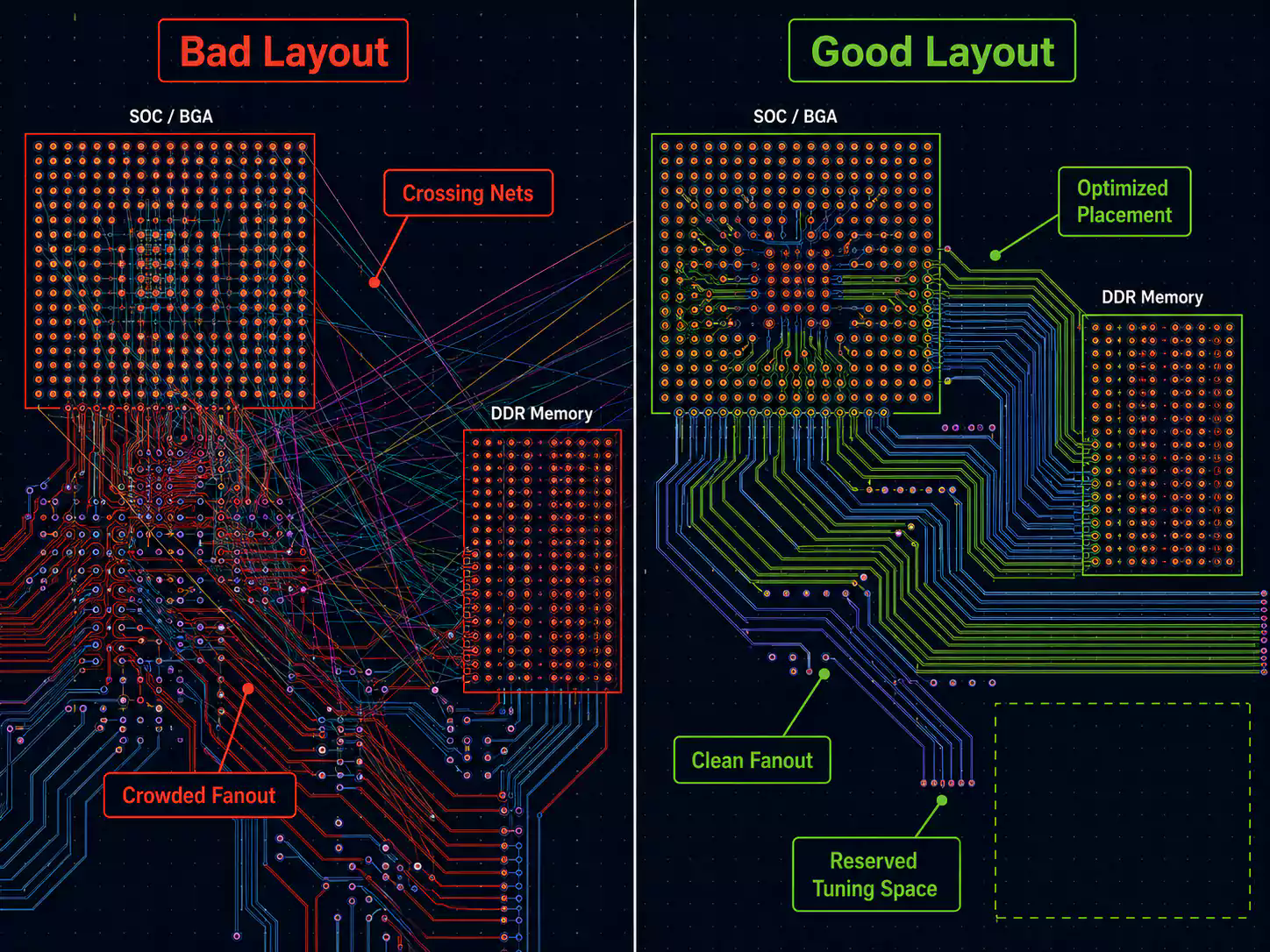
A placement that looks "tight and neat" but forces every byte lane through a via forest under the SoC is still a bad start. Distance is only one axis; orientation and channel ownership matter as much.
Stackup and impedance with the fab before routing
Confirm the stackup with the fabricator before you commit trace widths. Dielectric thickness, copper weight, and which layers sit against continuous ground decide whether a target impedance is manufacturable at a width that still escapes a fine-pitch BGA. For many DDR4-class interfaces, datasheets and controller guides cite common single-ended targets near about 40 ohm and differential targets near about 80 ohm. Those numbers are controller- and DRAM-dependent -- often selectable with drive strength and ODT -- not XFPCB guarantees. Put the actual targets from your SoC and memory documentation on the fab drawing, with layer assignment and tolerance, and ask CAM whether the proposed stack can hit them without absurdly wide or narrow copper.
Six-layer boards can carry some SoC-to-DDR layouts; not every six-layer recipe can. You need enough signal layers for byte-lane grouping, continuous reference under the data bus, and power distribution that does not steal the return plane. If an inner impedance layer needs traces so wide that the BGA pitch cannot host them, the stackup is wrong for that package -- fix it in conversation with the fab, not with creative neckdowns after escape.
Spacing practice taught across DDR4 routing guidance scales to the dielectric height H to the nearest solid reference: more clearance around CLK pairs (often cited around 5H in conservative guides) and somewhat tighter but still controlled spacing for ADDR/CMD and DQ groups (often around 3H). Solid, unbroken ground under the data region is non-negotiable. Plane splits under DQ or DQS are a classic bring-up killer that length reports never catch.
Fanout choice: dogbone, microvia, or via-in-pad
Decide the escape structure before you route the bus. Dogbone fanout on through vias remains the cost-effective default when BGA pitch and layer count allow clean channels. Through vias are easy to fabricate but can plug routing alleys on dense maps. Microvias on HDI stacks reclaim channel space when pitch and density demand it. Via-in-pad filled and plated (VIP) buys the densest escape when the ball map leaves no room for dogbones -- at higher fab and planarization cost.
Pick one primary strategy per DDR region and stick to it. Mixing VIP on one byte lane and deep through-via dogbones on the next produces via-count and stub skew that length matching cannot honestly repair. Tell the fab early: pitch, whether VIP or stacked microvias are required, fill/plate/planarize notes, and which layers own the first escape. That conversation belongs next to the impedance discussion, because both change the traveler and the quote.
Group routing: byte lanes first, DQS and CLK at the front of the queue
Route DDR as named groups, not as a bag of nets. Typical classes are DQ/DM, DQS (diff), CLK (diff), address/command, control, and power/ground. Within each byte lane, keep DQ and DM on paths that share direction, layer usage, via count, and reference with their DQS. Crossing byte lanes for "shortcut" copper is how DQS-to-DQ matching turns into a weekend of manual cleanup.
Prioritize DQS and CLK. Route the differential strobe and clock pairs first on clean corridors with consistent spacing, minimal vias, and continuous reference. Then pull the related DQ/DM of that lane alongside. Address and command groups follow their own matching rules -- often to CK -- and those skew budgets are typically much looser in absolute length than DQ-to-DQS matching inside a lane. Confusing those orders of magnitude is a common CAD mistake: over-tuning ADDR while under-protecting byte-lane consistency.
Keep the same layer plan for a given group where the controller guide allows it. Layer changes add via discontinuity and delay; when a change is required, add nearby ground vias so the return path follows. Continuous GND under the data region remains the rule of thumb taught in DDR4 length-matching and spacing practice -- break it and the eye diagram usually tells on you before the length report does.
Length matching as the last disciplined step
Only after placement, stackup, fanout, and group routing are stable should you open the length-tuning tools. Match within the rules the controller and DRAM specify: intra-pair skew on DQS and CLK as tight as the datasheet demands; DQ/DM to DQS inside each byte lane to the stated budget; ADDR/CMD/CTRL to CK to their (usually larger) budget. Tune in reserved pockets with controlled serpentine -- not in leftover scraps between via fields -- so coupling stays predictable.
If the board has no space left for tuning, the earlier steps failed. Dense accordion forced into a choked channel raises crosstalk and can undo the SI margin you thought you bought with "perfect" mil matches. Revisit placement or layer assignment rather than celebrating a length report that required heroic copper.
What DFM asks for on DDR jobs
From the fab and CAM side, a DDR RFQ that survives first-pass review reads like an interface package, not a generic multilayer order. Call out controlled-impedance targets and tolerances by net class or layer, with the stackup table and copper weights attached. Name the reference planes under the DDR region and state that those planes must remain continuous -- no splits under DQ/DQS/CLK. Describe BGA pitch and the agreed fanout: dogbone through-via, microvia HDI, or filled VIP, including any via-fill and planarize requirements. Note layer restrictions for byte lanes if your rules lock groups to specific layers. Include via limits on DQS and CLK if the design guide caps them. Attach the same Gerbers, fab drawing, and drill chart you would for any multilayer job, plus enough floorplan context that CAM can see why an impedance width or VIP callout is not optional decoration.
When those items arrive early, XFPCB can confirm whether the stack and via structure are buildable at the quoted capability before the layout team spends a week on serpentine that the board geometry cannot honestly support. Length matching still matters -- it is simply the last step that only works when placement, stackup, fanout, and group routing already earned the right to be tuned.