
The microsection comes back after lead-free reflow on a thick multilayer: a hairline crack in the inner-layer copper next to a PTH, or an IST coupon that fails early on the same stack. CAM did not change ounces. The laminate CTE in Z still pushed. What failed the stress test was foil ductility at temperature--not the line width the buyer argued about in layout review.
This article is for engineers specifying multilayer and HDI foil when thermal reliability and fine-line yield both matter. It is not the ED-versus-RA RFQ primer. Here the shop questions are Grade 3 HTE as a stress absorber near PTHs, when low-roughness or RTF is worth the peel trade, how high-performance resins change bonding beyond tooth height, and how CAM reads foil callouts on a stackup.
HTE Grade 3 as the stress absorber near PTH
IPC-4562 Grade 1 is standard electrodeposited foil. Grade 3 is High Temperature Elongation (HTE). The practical difference shows up at elevated temperature, not only at room-temperature tensile numbers.
During lamination presses and lead-free reflow, the dielectric expands in Z. That motion loads the copper at the edge of the plated through hole. Foil that goes brittle at high temperature cracks or separates; foil that still elongates absorbs the strain. Gould-class HTE notes call this out directly: elevated-temperature ductility resists foil cracks near PTH under Z-expansion. Variants aimed at dense MLBs sometimes advertise minimum elongation around 6% at elevated temperature for higher layer-count builds.
Shop ballpark numbers buyers can verify on laminate/foil datasheets (not XFPCB "certs"):
| Source context | Useful check | Typical guidance |
|---|---|---|
| IPC-4562 Grade 3 HTE | Prefer for multilayer | Grade 1 may pass simple boards; Grade 3 is the MLB default |
| Ventec HTE (CCP) style sheets | Elongation at 180 C | Often >=2% to >=3% by weight (e.g. thin foils >=2%, 18/35 um often >=3%) |
| Same sheets | Matt-side Rz | Standard HTE tooth often <6 to <10 um class by weight--not VLP |
| Gould JTCHTE / JTCHTEVLP notes | HTE + VLP split | HTE for PTH crack resistance; VLP for HDI / thin inners; etch factor ~3+ claimed on low-profile grades |
If your stack is thick, resin-rich, or runs multiple reflows, "1 oz copper" without Grade 3 / HTE language leaves the mill free to ship Grade 1 where HTE was assumed. For multilayer, CAM treats HTE Grade 3 as the baseline unless the drawing says otherwise.
Copper teeth vs fine-line etch and impedance
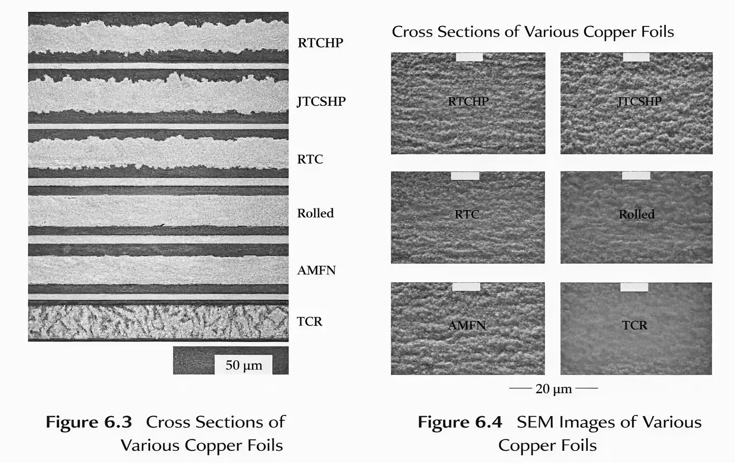
Standard-tooth HTE solves thermal ductility. It does not solve fine-line geometry. Matte-side nodules ("copper teeth") bite into thin dielectric and smear etch undercut. Results on the traveler:
- Trace edge distortion when L/S sits near the tooth height
- Local dielectric thickness scatter on thin cores
- Impedance coupons that wander because geometry is no longer the rectangle in the SI model
- In worst cases, tooth peaks from both faces of a thin dielectric that leave little resin between peaks
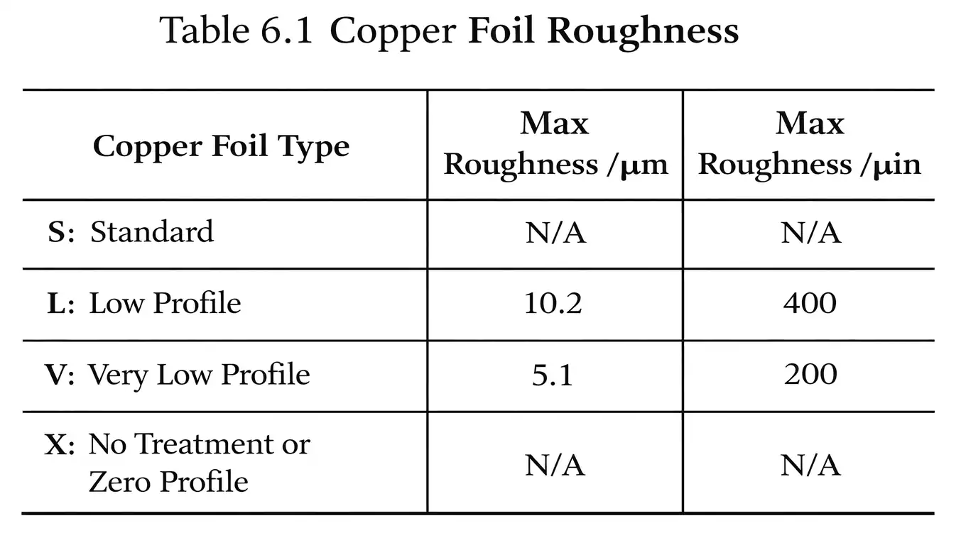
Roughness language in fab notes should use Rz (or Sq) on the face that bonds or that faces the critical dielectric--not a vague "smooth copper." IPC-4562 profile ladder (STD / LP / VLP / HVLP) is the shared vocabulary. VLP is commonly defined with matte-side Rz under about 5.1 um; practical VLP often lands nearer 2.5-4 um. Gould JTCHTEVLP is the Grade 3 + VLP combination aimed at HDI packages and thin inner layers, with etch-factor benefits versus standard tooth.
| Need | Foil posture | Why |
|---|---|---|
| Thick MLB, few reflows, wide lines | HTE Grade 3, STD or LP OK | Ductility first; tooth not the limiter |
| Fine inner L/S on thin cores | HTE + VLP (or RTF) | Tooth height eats etch factor and Dk thickness |
| Impedance-critical thin dielectric | Cap Rz on laminate face | Geometry and effective dielectric both move with tooth |
| HDI microvia / dense BGA fanout | HTE VLP on critical inners | Same as Gould VLP use case: thin inners + etch speed |
Do not buy VLP and then leave the stack on commodity tooth elsewhere without saying which layers matter. Call foil by layer or by net class.
RTF: adhesion / smoothness compromise
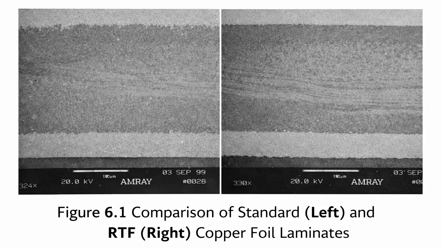
Reverse Treated Foil (RTF / DSTF family) keeps electrodeposited copper but flips which face gets the bond treatment. The smoother (drum) side is treated and laminated to the dielectric; the matte side faces outward for imaging adhesion.
Shop meaning:
- Laminate face stays low-roughness for fine-line etch and lower conductor intrusion into thin resin
- Outer face still has tooth that helps photoresist grab during inner-layer imaging
- Some processes reduce or skip aggressive inner-layer roughening--yield depends on cleanliness and resist system
RTF is the compromise when you need HTE ductility and a smoother bond face without jumping to exotic HVLP lead times. Peel is usually a bit lower than classic STD-tooth HTE on the same resin. That is the trade, not a scrap defect. On the drawing, "HTE VLP or RTF equivalent OK" is language CAM can stock-match; "smooth copper" is not.
High-performance resin needs more than roughness
BT, polyimide, cyanate ester, and some high-Tg / low-Dk systems are less forgiving on peel and process chemistry than commodity FR-4. Dropping Rz alone does not fix bond. Mills and foil makers combine:
- Controlled nodular treatment for mechanical interlock without returning to STD tooth heights
- Coupling / primer chemistry at the copper-resin interface
- Foil grades marketed for "advanced bond" on high-Tg or low-Dk cores (check the laminate datasheet copper options--do not invent a brand lock)
When the stack uses these resins, ask the fab which foil treatment is qualified on that slash sheet, not only which profile code is cheapest. High elongation at 180 C still matters for Z-stress; chemical bond and peel after process matter for long-term delamination risk. Roughness, ductility, and resin compatibility are three dials--turning only the first one is how RFQs get silent peel failures after CAF or thermal stress screening.
How CAM reads foil callouts on the stackup
Incomplete notes become stock STD HTE (or worse, Grade 1) even when the SI model assumed VLP. Complete notes are short and sit next to the stackup table.
Minimum CAM can build without guessing:
- Grade / elongation class: Grade 3 HTE (or explicit "HTE per IPC-4562 Grade 3")
- Profile or Rz max on the critical face: VLP, RTF, or "Rz <= 5.1 um matte" / tighter if required
- Weight per layer: 1/3 oz or 1/2 oz inners, etc.
- Which layers: signal inners vs planes vs outer start copper
- Resin family note if BT/PI/low-Dk: "foil treatment per laminate datasheet / fab qualification"
CAM-ready notes are short stackup sentences. Call all inner signal layers as ED HTE Grade 3 VLP (or RTF) with start weight, allow HTE STD on planes if that is fine, and for impedance layers name the layer numbers with an Rz max on the laminate face plus peel confirmation on the named mid-loss core. For thick MLB (2.4 mm and up) or multiple lead-free reflows, require HTE Grade 3 with no Grade 1 substitution.
Avoid writing only "1 oz copper" on a fine-line or thick MLB job. Do not demand HVLP maximum peel and minimum Rz with no trade accepted, lock a single foil brand with no equivalent when lead time is tight, or assume the laminate default tooth matches your etch and IST assumptions.
When HTE grade, profile/Rz, and layer scope sit on the same sheet as the stackup, XFPCB CAM can match stock, flag indent VLP/RTF, and refuse quiet STD swaps. That is how PTH crack risk and fine-line yield stop fighting on the same panel.