
The RFQ asks for low insertion loss on a 10 GHz channel and also asks for "standard peel" with no foil note. CAM pulls the laminate the buyer named--and that CCL arrives with standard-tooth ED copper because that is what the mill stocks for that slash sheet. Simulation assumed a smoother conductor. Peel looks fine on the traveler. The channel loses a few tenths of a dB per inch that nobody budgeted. That is the loss-budget versus peel-strength tension on a real quote: smoother copper helps HF loss; toothier copper helps adhesion and is cheaper. If the drawing does not pick a side, the shop will.
This article is for overseas buyers and layout engineers who need ED versus RA without guessing, who must decide when VLP/HVLP/RTF is worth the cost hit, and who want fab notes that stop silent foil substitution. Shop language, not a foil catalog.
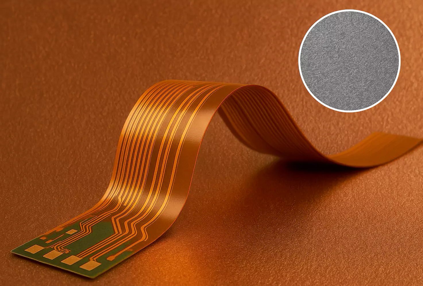
What "copper foil" means on a laminate datasheet
On a CCL or prepreg sheet, "copper" is not only ounces. Weight (1/2 oz, 1 oz) sets starting thickness. The foil type and profile set grain, roughness, and how the conductor behaves under bend and under skin effect.
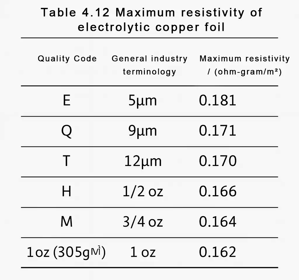
IPC-4562 frames metal foil for printed boards: purity, resistivity, type codes (ED Type E versus wrought/RA Type W), grades, and profile language. Untreated ED is typically specified around 99.8% copper (silver counted in copper); RA is often 99.9%. Resistivity limits differ by process--ED has tabulated maximums by weight; RA is generally in a tight ohm-gram/m2 band. Buyers do not need to recite the tables; they need to know that "1 oz copper" on a datasheet without profile still leaves the mill free to ship STD tooth when your model assumed HVLP.
Datasheet fields that actually change quotes:
| Field you see | Shop meaning | Silent-sub risk |
|---|---|---|
| Copper weight | Starting foil thickness before etch/plate | Low if weight is clear |
| Foil type ED / RA | Grain and flex story | High if blank on flex/RF |
| Profile STD / LP / VLP / HVLP | Matte-side roughness ladder | High on HF if only "1 oz" |
| Treatment / RTF / DSTF | Which face bonds, tooth orientation | Medium--RTF is not "same as STD" |
| Peel strength | Adhesion after process | Medium if you demand HVLP without peel check |
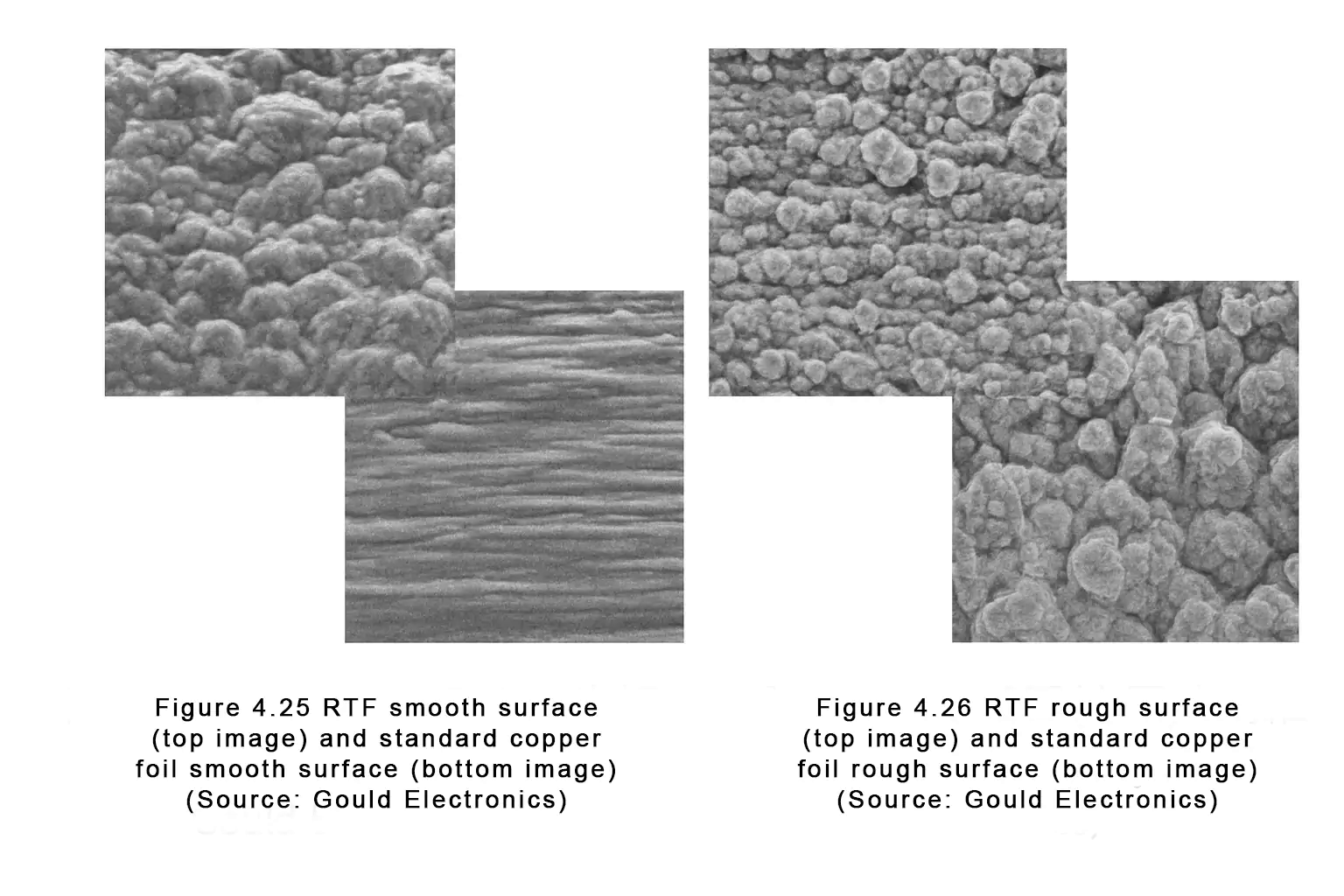
RTF (reverse-treated / DSTF family) is still ED: treatment sits so the laminate side is smoother for fine line and lower loss, while the outer face keeps tooth for later bonding. Peel is usually a bit lower than classic STD ED. That is a deliberate trade, not a defect.
ED vs RA decision tree from fab stock reality
Start from what the fab can pull this week, not from ideal physics.
ED (electrodeposited, Type E) -- Copper grows on a drum. Columnar grains run mostly through the thickness. Matte side is naturally toothy; drum side is smoother. Stock is wide, cheap, and default on rigid multilayer. Flex fatigue is poor relative to RA because cracks prefer vertical grain paths. HF loss tracks roughness: STD is fine below roughly 1 GHz on short routes; LP/VLP/HVLP climb the cost ladder as skin depth shrinks.
RA (rolled annealed, Type W) -- Ingot is rolled and annealed into pancake grains parallel to the sheet. Both faces start smooth; treatment is added for bond. Ductility and flex-cycle life jump by roughly an order of magnitude versus ED at the same weight and bend radius. Cost and lead time jump too; fewer mills, narrower rolls, more indent risk.
Practical tree CAM uses:
- Is any zone dynamic or static flex / rigid-flex bend? -> RA (or hyper-annealed RA for hinge-class dynamic flex) in flex copper. ED only in rigid zones if the construction allows hybrid foil.
- Rigid only, frequency and length leave loss budget comfortable with STD or LP ED? -> Stay on ED stock. Do not pay RA for a 100 MHz power/digital board.
- Rigid HF / SerDes where dielectric is already mid/low-loss and conductor loss still eats margin? -> Low-profile ED (VLP/HVLP/RTF) first. RA on rigid RF is a specialty call when Rz must sit near 1 um and the laminate family supports it.
- Buyer wrote only "1 oz copper"? -> Shop ships default ED for that laminate. Expect STD profile unless the CCL brand locks something else.
| Question | Prefer ED | Prefer RA |
|---|---|---|
| Board flexes in use or install | No (rigid) | Yes (flex zones) |
| Cost / lead time critical | Yes | Only if mandatory |
| Peel first, loss second | STD/LP ED | Treated RA still needs peel check |
| Loss first on rigid HF | HVLP/RTF ED | RA if model and fab agree |
When low-profile ED is enough vs when RA is mandatory
Roughness and skin depth decide the ED profile ladder. At 1 GHz skin depth in copper is about 2 um; at 10 GHz it is well under 1 um. When roughness peaks sit in the same neighborhood as skin depth, current rides the hills and conductor loss rises. Shop rule of thumb--not a substitute for your channel budget:
| Profile (ED) | Typical Rz ballpark | When it is usually enough |
|---|---|---|
| STD | ~5-8 um | Consumer / power / digital under ~1 GHz |
| LP | ~3-5 um | Mid-speed, Wi-Fi class, short HF |
| VLP | ~2.5-4 um | ~5-15 GHz / 10G-class with mid-loss dielectric |
| HVLP / many RTF | ~1.5-2.5 um | 25G-class, mmWave short routes on rigid |
Low-profile ED is enough when the board is rigid, peel must stay healthy for thin cores and thermal cycles, and the loss budget closes after you pick dielectric Df first. Many 5-25 GHz rigid jobs close on VLP/HVLP without jumping to RA--especially when trace length is short.
RA is mandatory when flex copper must survive bend cycles: static fold still wants RA; dynamic hinges want the ductile RA/HA end of the catalog. Cycle counts for ED at a tight radius often land in the low thousands to low tens of thousands; RA commonly lands one to two orders higher under comparable IPC flex fatigue checks. That is not a marketing delta--it is crack path physics.
Hybrid rigid-flex is normal: RA in flex layers, ED (even STD) in thick rigid sections to save cost. Call foil by zone. One global "copper foil: RA" on a mostly rigid board burns money; one global "ED" on a hinge board burns field returns.
Cost posture buyers should expect: HVLP/RTF ED often sits modestly above STD; RA is commonly a multiple of STD and may extend lead time. Paying for HVLP while leaving Df at commodity FR-4 can waste the foil premium. Paying for RA "for smoothness" on a non-flex digital board when VLP ED was enough is the same waste in the other direction.
Specialty foils when they actually show up
Most RFQs never see these. Spec them only when the process needs them.
Double-treated foil -- Bond treatment on both faces. Can skip some inner-layer roughening steps, but demands extreme surface cleanliness. Rare on everyday multilayer quotes; more a process option than a buyer default.
Resistive foil -- Alloy resistive layer on the copper so inner-layer etch can form embedded resistors. Shows up when discrete R count, space, or reliability pushes resistors into the stack. Needs laminate/process support and resistor design rules--not a note you add casually to a digital fab drawing.
Ultra-thin ED with carrier -- Foils around a few um travel on a thicker carrier, then the carrier peels after lamination. Packaging substrates and ultra-fine line work use this; commodity 1/2 oz and 1 oz jobs do not. If your HDI shop did not propose carrier foil, do not invent it on the RFQ.
DSTF/RTF sits between "specialty" and "everyday HF ED": for fine inner lines and lower tooth intrusion into thin dielectrics it is a mainstream HF choice, still with a peel tradeoff versus STD.
How to write foil lines on fab notes
Incomplete foil notes cause silent substitution. Complete ones are short.
Minimum that prevents the wrong tooth:
- Foil process: ED or RA (Type E / Type W language is fine if your team uses IPC-4562 codes)
- Profile or Rz max: e.g. VLP or Rz <= 2.5 um on the bonding face you care about
- Weight per layer or per zone: 1/2 oz inner, 1 oz outer, etc.
- Flex vs rigid zones on rigid-flex: RA in flex copper; ED allowed in rigid if true
- Whether RTF/DSTF is required or "HVLP or RTF equivalent OK"
CAM-ready notes look like short stackup sentences rather than a copper weight alone. For rigid HF, call signal layers by number with ED HVLP (or RTF), start weight, and an Rz max on the laminate face, while allowing ED STD on planes if that is acceptable. On flex, name RA copper treated for PI bond, and confirm RA/HA grade against the stackup for dynamic flex. On hybrid rigid-flex, keep ED HTE in rigid zones per the laminate and RA only in flex zones so ED is not substituted into the bend region.
Avoid writing only "1 oz copper" on an HF or flex job. Do not demand HVLP and maximum peel without accepting the tradeoff, lock a foil brand with no equivalent when lead time matters, or assume the laminate datasheet default matches your SI model.
When foil type, Rz cap, and zone rules sit next to the stackup and impedance table, XFPCB CAM can match stock, flag indent items, and refuse quiet STD swaps. That is how loss budget and peel strength stop fighting on the traveler.