
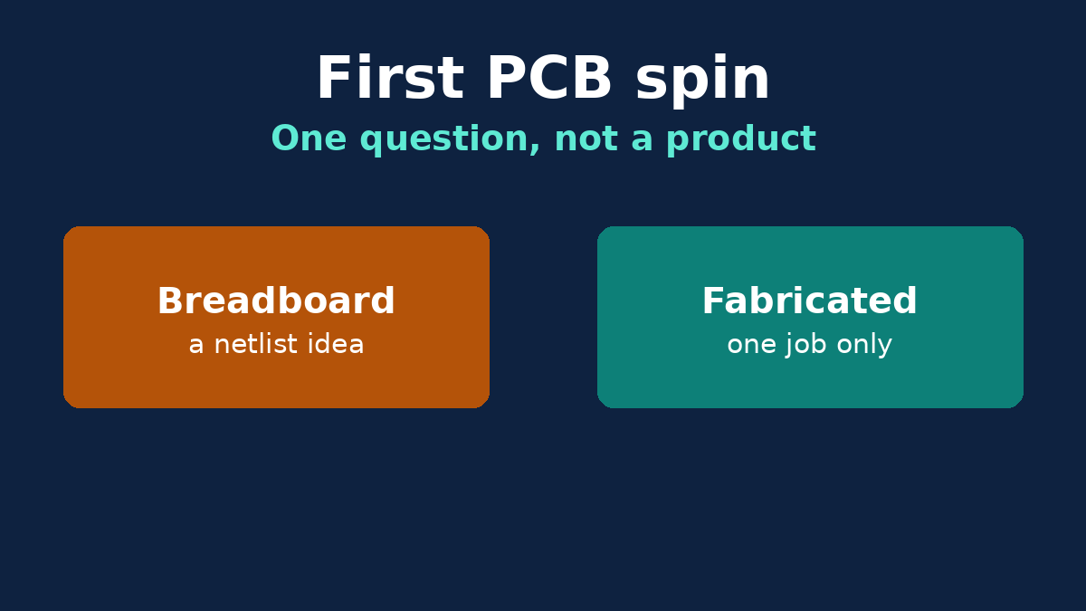
A circuit that works on a breadboard has answered a real question. It has not answered the question a fabricated board exists to answer. The gap between those two is where first-spin orders get loaded with production decisions the spin cannot inform, and then sit while someone debates a laminate the circuit does not use.
What the hand-built board is actually evidence of
A solderless breadboard lets you swap parts and see whether an idea does the thing. The wiring is long, the contacts are springs, and there is no ground plane. That is a feature while the schematic is still moving. It is also why the same circuit can misbehave, or behave too well, once it is a layout. Slow logic, a sensor bias, a power-up sequence: a breadboard can carry those. Edge rates, a switch-mode loop, creepage from mains copper to a connector shell, the height of a part under a lid: it cannot.
Perfboard and stripboard solder that idea down. They are more stable than springs, and they are still a hand routing. Stripboard in particular gives you copper strips you will not have on the PCB, and it withholds the plane you will. A board that works there is evidence the netlist is worth drawing. It is not evidence the drawing is right. Treat a request to "copy the perfboard" as a schematic, not as a Gerber.
None of this means throw the breadboard away. It means stop citing it as a revision of the PCB.
Give the first fabricated spin one job
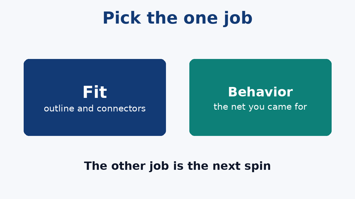
Write the job in the email, in one line. The spins that finish are usually one of these:
- Fit. Outline, mounting holes, connector facing, mating height, keep-out under the lid. The circuit can be a subset. A board that is electrically perfect and two millimetres too wide has failed the only test you paid for.
- Layout behavior. The loop, the ground, the connector pinout, the net that was noisy or hot on the bench. The enclosure can be approximate. A beautiful outline with the switch node routed as a long trace has also failed the only test you paid for.
Asking one spin to be both, and also the production panel, the impedance coupon program, and the cosmetic standard, is how a five-day question becomes a stackup meeting. Our PCB Prototype page is built around bring-up, enclosure fit and revision loops. Name which of those this order is. If the note does not say, the files will be reviewed as if all of them matter, including the ones you have not decided.
A later spin can take the other job. That is a second order, not a failure of the first.
What you can leave at the default
If the edges are slow, the product is not a flex, and you are not trying to prove a metal-base or a high-frequency stack, the first spin can be an ordinary rigid board. Say "standard FR-4, standard copper, a common finish" and spend the attention on the outline or the net. Opening a laminate comparison for a connector-fit board does not make the connector righter.
You can also leave off, unless they are the question:
- impedance control and coupons
- blind or buried vias
- a production panel with scoring and rails
- a debate about IPC class, when the spin is not about whether the fab held a tolerance
Class, coupons and a production array matter when you are checking the factory, or when the circuit will not work without them. They are not a courtesy you add because the file looks unfinished. A fit-check with a Class 3 note and no room for the annular ring that class implies will stall on a problem the enclosure cannot reveal.
What you must not simplify
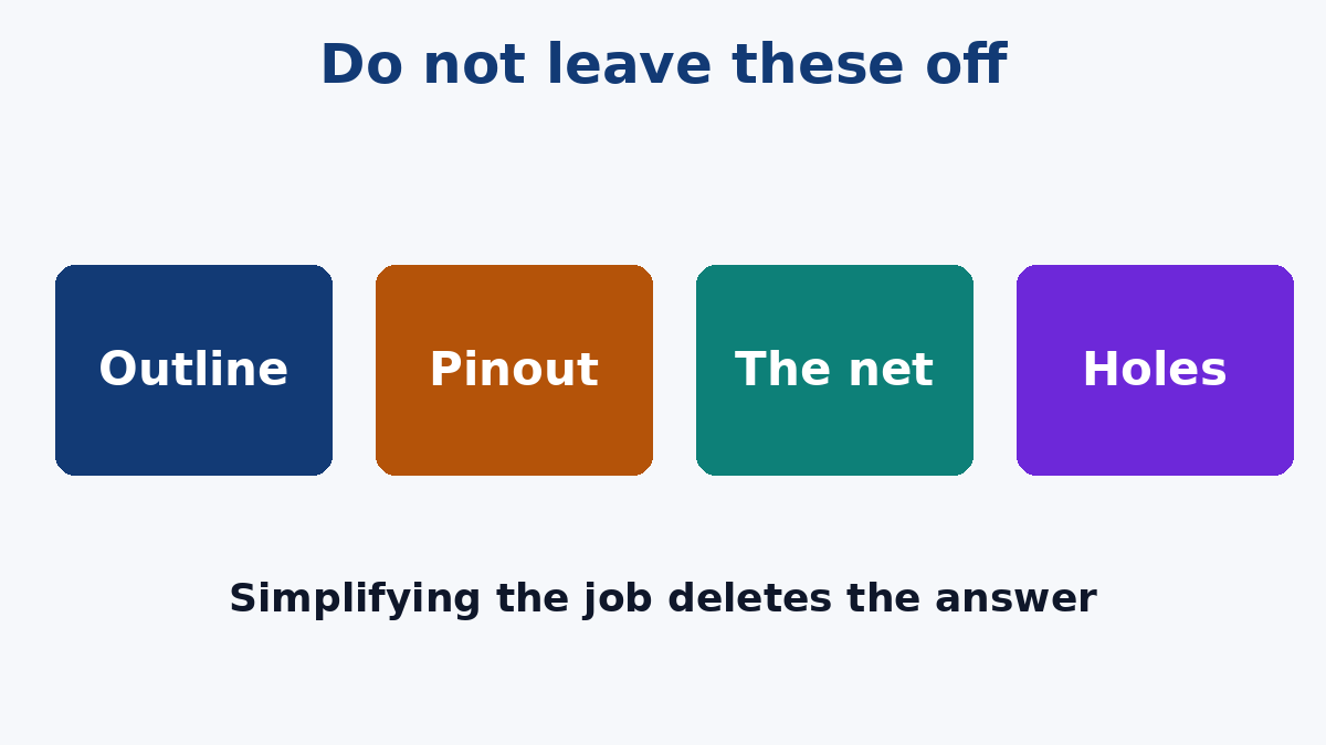
The things that make a spin worthless are the ones that were the job:
- Outline and holes, if the job is fit. Mounting holes in the wrong place are not a touch-up. They are a new board.
- Connector pinout and polarity, either way. A mirrored header is the classic "the perfboard had the pins facing me." Draw it from the mating part, not from memory of the breadboard.
- The net you came to see, if the job is electrical. Do not delete the switch node onto a convenient pour "just for the prototype" and then conclude the layout is quiet.
- Hole sizes for the mechanical parts you will actually insert. A display, a switch, a connector shell. Electrical nets can be a subset. The hole the switch does not fit through cannot.
Assembly is part of the spin only when the question needs parts on the board: firmware, a solder joint, a tall part under the lid. Our Prototype PCB Assembly page is the small SMT and through-hole lot for that, aimed at fit, firmware and test coverage before a production revision. A bare board is enough when you are checking outline, holes and a connector footprint with a mating plug. Do not add a BOM to a fit-check that you could have answered with a ruler and the real connector.
The file set for this spin, not the next one
Enough to build, and no more than the question needs:
- Gerbers and drill, with the outline on its own layer
- board thickness, layer count, copper, and the finish, in one note
- which question this spin is answering
- if it will be assembled: BOM with manufacturer part numbers, pick-and-place, and polarity on the drawing
A stackup essay, a panel drawing, and a test-procedure for a product you have not powered yet can travel with the second spin. Sending them now does not make the first answer more trustworthy. It makes the first answer wait.
The breadboard can stay on the bench for the nets you are still changing. The fabricated board should be aimed at the one thing the breadboard was never going to show you.