
The return came back with an intermittent open that only showed after thermal cycling. Continuity on the bare board had passed. Under the microscope the via barrels that linked top copper to bottom copper looked plated, but the wall thickness at mid-barrel was thin enough that Z-axis expansion cracked the copper on the second or third temperature swing. That failure mode is why double-sided boards live or die on plated through-hole quality, not on how neat the outer traces look in Gerber.
Buyers and designers choosing between single-sided, double-sided, and multilayer constructions keep hitting the same China-fab hinge: when FR-4 with copper on both sides and solid PTH is enough for the industry application, and when the product forces multilayer planes or a metal-core path instead. This article stays on that materials and reliability cut.
What "double-sided" means in materials terms
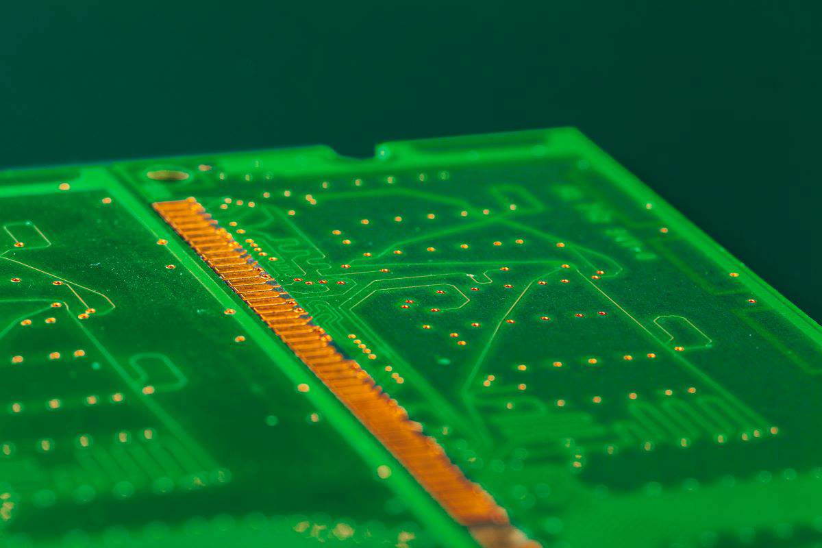
In laminate language, a double-sided PCB is a copper-clad laminate with copper foil bonded to both faces of an insulating core -- most often FR-4 glass-epoxy. The stack, simplified, reads solder mask, top copper, FR-4 core, bottom copper, solder mask. There is no inner copper foil buried inside the core the way a four-layer or higher build adds prepreg and additional signal or plane layers.
That materials picture explains the capability jump over single-sided boards without pretending the board is multilayer. Single-sided constructions put copper on one face only; crossovers need jumpers or creative routing that burns area. Double-sided constructions put usable routing on both faces, so a net can leave a pad on the top, drop through a via, and continue on the bottom without enlarging the outline. Density rises. Cost stays below multilayer lamination for many industrial and commercial jobs that do not need buried planes.
FR-4 CCL with copper on both sides is the default starting material at China fabs for this class of work. Copper weight is commonly 1 oz (about 35 um) per side for digital and mixed-signal boards; 2 oz shows up when power traces need more cross-section. Finished thickness often lands near 1.6 mm for connector and chassis compatibility, with thinner and thicker cores available when aspect ratio and mechanical constraints allow. High-Tg FR-4 becomes a materials call when the board will see two lead-free reflow passes for double-sided SMT and standard Tg would sit too close to the thermal budget.

How PTH turns two copper faces into one circuit
Two copper foils on opposite faces of FR-4 are still two separate conductors until a plated through-hole joins them. A via is drilled through the full board thickness. After cleaning, electroless copper deposits a thin seed on the non-conductive hole wall -- typically on the order of a fraction of a micron to about one micron -- so the barrel can take current in the electrolytic tank. Electrolytic plating then builds the barrel wall to the specified thickness. IPC-6012 Class 2 guidance commonly treats about 18 um average copper wall as the reliability floor many fabs quote for production boards; thicker walls improve margin against thermal fatigue.
That copper-lined barrel is the only interlayer link on a true two-layer board. There are no buried vias and no blind vias in the multilayer sense, because there are no inner layers to land on. Every interlayer connection is a full-thickness PTH. Aspect ratio -- board thickness divided by drill diameter -- controls how evenly plating can throw into the barrel. A 1.6 mm board with a 0.3 mm drill sits in a comfortable plating window for most China process sheets. Push the drill much finer on the same thickness and the center of the barrel starves, which is exactly the thin-wall intermittent that opened this article.
Via geometry also includes the annular ring: copper pad remaining around the drilled hole after registration and tolerance stack-up. Thin rings tear or open under drill wander and thermal stress. Current through a single via is limited by finished hole size and plating; parallel vias share load on power nets more safely than one oversized hole that pushes aspect ratio into the danger zone.

Fab steps that decide yield on both sides
Yield on double-sided boards tracks a short list of process steps that single-sided work can skip or soften.
Drill quality comes first. CNC drilling creates vias, component holes, and mounting holes in one pass through the CCL. Debris left in the barrel contaminates subsequent metallization. Drill wander eats annular ring. Aspect ratio that the process sheet cannot plate cleanly becomes a field risk even when electrical test on the bare board still reads continuous.
Electroless copper seed follows cleaning and activation. Without a continuous seed on the glass-epoxy wall, electrolytic copper cannot build a reliable barrel. Poor adhesion or incomplete coverage shows up later as barrel cracks and intermittent opens after thermal cycling -- often after the board has already left the fab.
Electrolytic plating builds wall thickness and surface copper. Throwing power, bath chemistry, and current density decide whether small holes meet the Class 2 average wall target across the panel. Thin mid-barrel plating is a process problem, not a layout mystery.
Imaging and etch run on both sides. Photoresist defines the circuit pattern; etch removes unwanted copper while plated traces and barrels remain. Because both faces are patterned, registration between top and bottom artwork matters for pads that share a via. AOI against the Gerbers catches opens, bridges, and copper defects before mask and finish.
Solder mask, surface finish, and silkscreen close the fab sequence. Finish choice (HASL, ENIG, OSP, and others) interacts with double-sided SMT thermal cycles: the secondary side sees heat again when the primary side reflows. Electrical test still verifies net continuity and isolation; it does not replace thermal-stress screening when via plating is marginal.
Where two layers win -- and when industry apps force more
Double-sided FR-4 wins when the circuit needs denser routing than single-sided can deliver, yet does not require buried power or ground planes, tight controlled impedance across many high-speed nets, or a dedicated metal thermal path. Power supplies, industrial control interfaces, LED driver boards on FR-4, automotive body electronics of moderate complexity, hard-drive and consumer modules, and many IoT products sit in that band. Versus single-sided, two copper faces cut jumpers and shrink outline. Versus multilayer, the fab avoids inner-layer lamination, so cost and lead time stay lower for the same outline when planes are not mandatory.
Industry applications push past two layers when return-path integrity and EMI compliance need a solid plane that a fragmented bottom pour cannot provide, when controlled-impedance tolerance tighter than a two-layer microstrip can hold is on the critical path, when component density drives features below what a two-layer process window can plate and etch at volume, or when PDN performance needs distributed plane capacitance. Metal-core constructions (aluminum or copper core) enter when LED arrays, power converters, or similar loads need a short thermal path that FR-4 dielectric cannot match. In those cases the materials decision is not "more copper on FR-4 faces" -- it is a different stack family.
The China-fab view stays practical: quote two-layer FR-4 with documented PTH capability when the schematic and EMI plan fit that construction. Escalate to four-layer or metal-core when the failure modes you care about are plane integrity, impedance control, or heat -- not when the only pressure is habit.
RFQ notes that lock PTH and assembly intent
A double-sided RFQ that CAM can build without guessing states copper weight per side, finished board thickness, minimum finished hole size and via aspect ratio assumption, IPC class (Class 2 versus Class 3 annular ring and acceptance), surface finish, and whether SMT lands on one side or both. Both-side SMT implies two reflow passes: call out side assignment expectations for heavy parts and any adhesive or process notes your EMS already locked. Via-in-pad under QFN or similar pads needs fill and cap called out if that is the design; open vias in solder pads wick paste.
Attach Gerbers or ODB++, drill files, and a short fab note that names FR-4 (and Tg if high-Tg is required), copper weight, hole list, and electrical-test expectation. XFPCB quotes from that package so plating capability, etch rules for the stated ounces, and assembly sequencing align with the two-layer materials story instead of a silent upgrade to multilayer mid-quote.
Two copper foils on an FR-4 core become one reliable circuit only when the PTH barrel survives the thermal life the product will see. Choose double-sided when that materials stack matches density and cost; move to multilayer or metal-core when planes or heat demand a different construction -- and write the RFQ so copper weight, hole size, IPC class, and both-side SMT intent are explicit before CAM starts.