
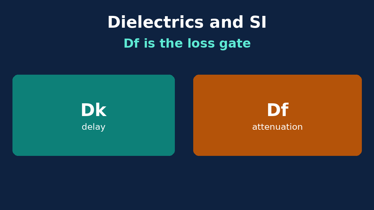
High-speed links fail the eye when the channel eats the edge. Part of that channel is the dielectric between and around the copper. Dk sets how fast the wave travels and how wide a trace must be for a target impedance. Df (dissipation factor) sets how much energy the resin/glass absorbs as heat—especially in the harmonics that make a fast rise time.
This post is the material gate for overseas buyers and engineers: when FR-4-class dielectrics are still honest, and when low-Df becomes a stack requirement. It is not a brand Gbps menu, not a full channel-loss lever map, and not the single-vs-multi-sheet prepreg construction post.
Rise time sets the frequencies you must keep
A digital edge is not a single sine. Shorter rise time means more high-frequency content. A common rule-of-thumb bandwidth scale is on the order of 0.35 / rise time (with rise time in ns giving GHz-scale bandwidth)—useful for intuition, not a law to paste into every RFQ. If the dielectric attenuates those harmonics, the edge slows and the eye closes.
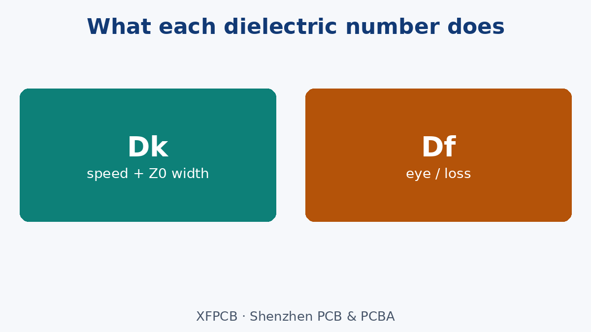
What Dk and Df each buy
- Dk: delay, impedance geometry, timing skew between paths in different dielectrics.
- Df: dielectric attenuation along the path; dominant softener of the eye when paths are long and rates are high.
- Frequency stability of both: whether your simulation and the fab’s coupon speak the same language—state frequency and test method on datasheet comparisons.
Conductor loss still shares the budget
Dielectric loss is only half the story. Skin-effect conductor loss and foil roughness join at GHz. Widening a trace can trade density for lower conductor loss; it does not delete a high-Df dielectric on a long path. The copper-roughness stack-note post owns foil grade; here the gate is whether the resin system itself is the remaining lever after geometry is reasonable.
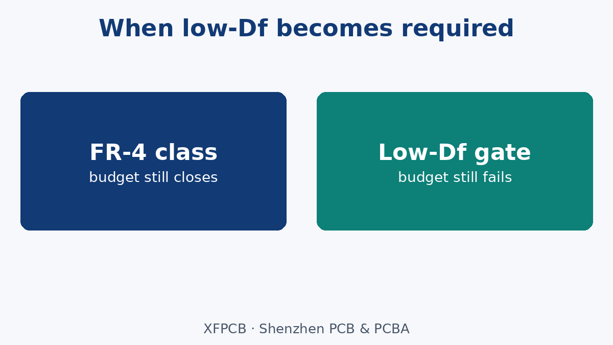
When FR-4-class is enough
Short nets, modest edge rates, and loss budgets that still close with standard laminates do not need an exotic resin by default. Pay for process control, impedance callouts and clean vias before you pay for Df you do not need.
When low-Df becomes a gate
Long backplanes, multi-Gbps chip-to-chip paths, and RF lines where measurement already shows dielectric loss dominating—then name a low-Df family (or “fab equivalent meeting Df ≤ … at f”) on the stack. Do not paste a brand from a blog chart. Confirm availability and hybrid rules with the fab.
Eye diagrams and BER are system checks. A closed eye can be vias, connectors, crosstalk or dielectric. Material upgrade without a budget is hope.
What to write on the RFQ
- Which nets are SI-critical and their approximate edge/rate class (without inventing a mandatory Gbps table).
- Laminate family or Df/Dk targets at a stated frequency.
- Impedance and coupon expectations.
- Whether hybrid (FR-4 + low-loss islands) is allowed.
Our High Frequency PCB and Impedance Control PCB pages are the construction and measurement seats.
What we are not claiming
No Megtron/Rogers bake-off, no invented dB/m limits, no claim that low Dk alone opens every eye, and no replacement for channel-loss or foil-roughness posts. Use rise time and loss budget to decide whether Df is a material gate. Then name the dielectric honestly on the stack.