

An open circuit on a returned board is one of the most common reasons a buyer opens a quality claim, and one of the easiest to mishandle. The board is often reworked on the bench, jumpered, flexed, or cut before anyone has recorded where the failure actually is. By the time it reaches the factory, the evidence that would separate a fabrication defect from an assembly defect or a field-stress failure is gone. Repair guides tell you how to bridge a broken trace. This article is about the opposite job: how to localize an open without destroying it, how to tell which process step most likely created it, and what to put into an 8D or RMA request so that the corrective action you receive is about your failure rather than a generic letter.
We write from the factory side. At XFPCB we run bare-board fabrication and PCBA under one roof, so we see the same open from both ends: the bare-board electrical test record, the assembly profile, the X-ray image, and the microsection. The patterns below are the ones that decide whether an investigation closes in a useful way or stalls in a dispute about who caused what. If you want the background on the typical root causes themselves, our earlier post on open circuit root causes in fab versus assembly covers that ground; here we focus on localization, evidence handling, and the request you send.
Why "open circuit" is not yet a failure description
"Open on net VCC_3V3" tells a factory almost nothing. An open can sit in at least five physically different places, and each one points to a different process owner:
- In the copper conductor itself – an etched-through trace, a nick from handling, a scratch through mask and copper, or an inner-layer conductor broken during lamination.
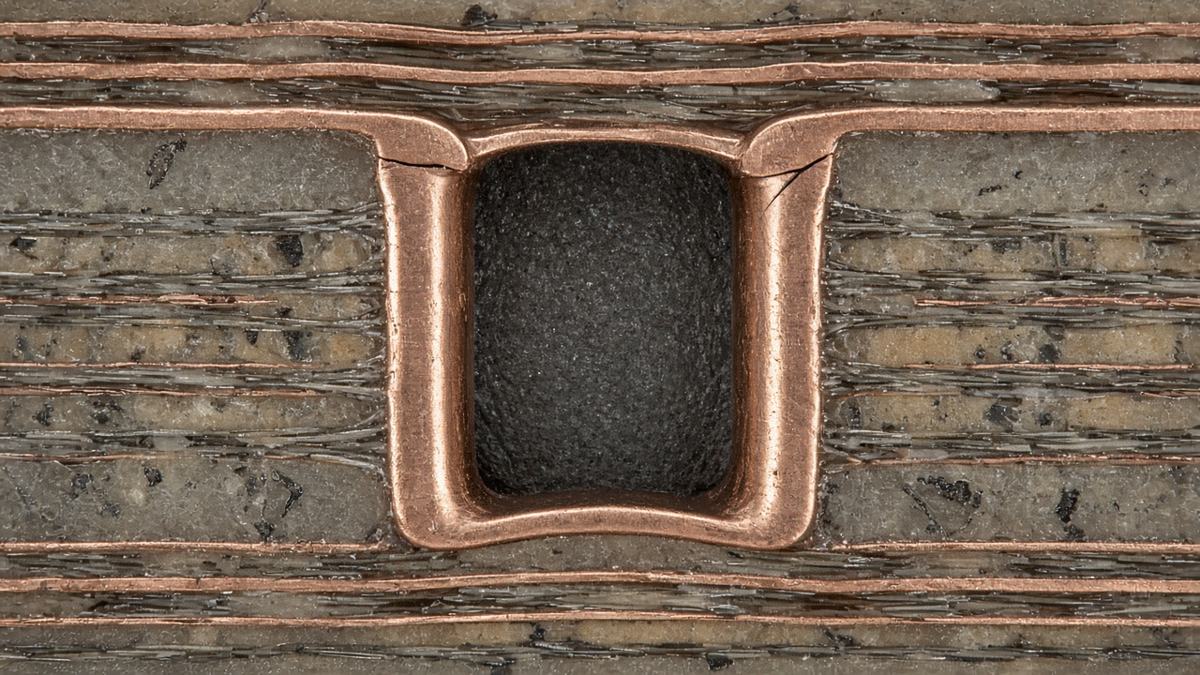
- At the via or plated through-hole – a barrel crack, a plating void, a corner crack at the knee, or a separation between the barrel and an inner-layer pad (an interconnect defect).
- At the pad-to-laminate interface – pad cratering under a BGA or a lifted land after rework, where the copper pad has torn away with or from the resin beneath it.
- In the solder joint – non-wetting, head-in-pillow, insufficient paste, a cracked fillet from thermal cycling, or a lifted lead on a fine-pitch package.
- Inside the component – a cracked MLCC, an open bond wire, a damaged connector contact, or an internal fuse that did its job.
The first two are almost always fabrication-related, the fourth is almost always assembly-related, and the third and fifth can be either, depending on design, handling, and thermal history. A meaningful failure description therefore names the net, the two end points that measure open, the location narrowed down as far as non-destructive methods allow, and the condition under which the open appears (always, hot only, cold only, under flexing, after a specific number of cycles).
Step one: preserve the evidence before you touch it
The single most expensive mistake in open-circuit handling is bench rework before documentation. Reflowing a suspect BGA "to see if it fixes it" may close a head-in-pillow joint and destroy the evidence; it may also open a marginal via barrel that was not the original defect. Before anyone applies heat or a probe with force, we recommend:
- Photograph both sides of the board under even lighting, plus close-ups of the suspect area. Record serial number, date code, and lot marks from the board and any labels.
- Record the history. How many reflow passes did the board see, including rework? Was it conformally coated? What temperature cycling, vibration, or drop exposure has it had in the field? How many hours or cycles before failure?
- Quarantine and bag the board in ESD-safe packaging with the history sheet. Do not wash, re-coat, or bake it unless asked.
- Keep sister boards. A failed board plus two or three passing boards from the same lot are worth far more to a failure analyst than five failed boards with no reference.
- Do not remove components near the suspected location without recording why and how. If removal is unavoidable, note the method and temperature.
This list costs almost nothing and is often what decides whether the 8D can identify a root cause at all.
Step two: electrical localization without cutting
Most opens can be localized to within a few millimeters electrically, before any destructive work. The goal is to shrink the search area so that the eventual cross-section lands on the defect rather than next to it.
Low-resistance and four-wire measurements
A continuity beep only tells you that resistance is below a threshold. Intermittent and partial opens hide above that threshold. Use a four-wire (Kelvin) resistance measurement between nodes along the net and compare with the same net on a known-good board. A via chain or trace that reads higher than its twin on a good board is a candidate even if it still "beeps." Record values; a table of resistances along the net is a useful attachment to the RMA.
Node-by-node splitting
Use the netlist and layout to identify every accessible node on the failing net: component pads, test points, vias with exposed annular rings, connector pins. Measure from one end and move along the net until the open appears between two consecutive nodes. The defect sits somewhere in the copper and vias between them. On multilayer boards, the layout will tell you which layers and which vias the path uses between those nodes, which immediately suggests whether you are hunting for a trace, a via, or a joint.
Thermal and mechanical sensitivity
An open that appears only when the board is warm or only when it is bent is a valuable clue. Barrel cracks and interconnect separations often open at elevated temperature as the laminate expands in Z and close again at room temperature. Cracked solder joints and cracked ceramics often respond to gentle flexing. Use a controlled method—a hot plate set to a stated temperature, a heat gun at a fixed distance with a thermocouple, or a freeze spray—and record which stimulus opens the circuit and which closes it. A statement such as "net opens above approximately the board's operating temperature, closes on cooling, localized between via cluster U5-A and pad R12.1" is the kind of description that lets a factory pull the right lot records.
X-ray and optical inspection
Once the area is narrowed down, X-Ray Inspection can show solder voiding, missing balls, bridging, and gross barrel defects, while angled optical inspection shows lifted leads and fillet cracks. X-ray is not a microsection: it rarely resolves a hairline barrel crack or an interconnect separation, and a clean X-ray does not clear the via. Treat it as a way to rule assembly causes in or out at a joint, not as proof that the bare board is good.
Step three: decide fab, assembly, or field before destructive analysis
With the open localized, you can make a working hypothesis about the process owner. We use a simple decision frame internally.
| Localized to | Typical owner hypothesis | What usually confirms it |
|---|---|---|
| Surface trace with visible damage | Handling or field mechanical damage, sometimes fab | Damage morphology, mask condition, location vs fixtures |
| Inner-layer conductor between two vias | Fabrication | Bare-board test record, cross-section of the conductor |
| Via barrel, opens hot | Fabrication (plating or drilling), aggravated by thermal history | Microsection showing crack, void, or separation location |
| BGA or fine-pitch joint | Assembly (paste, profile, warpage), sometimes pad finish | X-ray, dye-and-pry or cross-section, finish analysis |
| Pad torn from laminate | Mechanical stress, rework, or laminate/pad design | Cross-section showing crater in resin under pad |
| Inside component | Component or assembly stress | Component-level analysis, supplier involvement |
This is a hypothesis, not a verdict. Its value is that it tells you which records to request and which analysis to order first. Asking a bare-board supplier for an interconnect cross-section when the evidence points to a cracked MLCC wastes everyone's time and delays the real corrective action.
The bare-board electrical test record matters
Every production bare board that ships with electrical test has a test record or at least a lot-level pass. If your board was tested with Flying Probe Testing or a fixture test against the netlist, an open that is present on the bare board at room temperature should have been caught. A room-temperature open found after assembly therefore points either to a test escape (rare, but it happens, and it is worth asking about) or to a latent defect that only opened under assembly heat. That distinction is important: a latent barrel or interconnect defect is still a fabrication root cause, but its corrective action is about plating, desmear, and reliability coupons, not about the electrical tester.
Step four: destructive analysis that answers the question
When the open is localized to a via, a joint, or an inner conductor, a microsection is usually needed. Microsections are irreversible, so plan them.
- Section the right feature. Mark the exact via or joint on a photo and in the request. Sectioning "near U5" is not enough; a section a millimeter away from the defect shows a perfect via.
- Section a reference. Ask for an equivalent via or joint from a passing board, or an adjacent passing via on the same board, to be sectioned in the same way.
- Ask for unetched first. Interconnect defects are confirmed on polished, unetched specimens; etching can create interface lines that look like separations. A good report states whether the sample was etched and shows both conditions when relevant.
- Consider horizontal sections for barrel-to-inner-layer questions. A vertical section shows two points of the barrel wall; a horizontal section at the inner layer shows the whole ring of the connection.
- Use dye-and-pry for area arrays when you need to know how many BGA joints were cracked or never wetted, but remember it destroys the package interface and cannot be combined with sectioning those same joints.
- SEM and EDS are worth requesting when contamination, residue, or an unexpected finish interface is suspected. They are slow and should follow, not replace, optical sectioning.
The microsection should report what IPC-A-600 inspection practice calls for at that feature: plating thickness at the barrel wall and knee, any voids, cracks and their location, inner-layer connection condition, resin recession, smear or etchback condition, and laminate condition around the hole. If you buy to a performance class under IPC-6012, ask that the observations be compared against the acceptance criteria for that class, rather than described in general terms.
Common open-circuit failure modes and their fingerprints
Knowing the fingerprints helps you write a better request and judge the answer.
Barrel cracks usually run circumferentially in the middle of the barrel or at the knee where the barrel meets the outer land. They are driven by Z-axis expansion of the laminate during reflow and thermal cycling, and aggravated by thin or brittle plating, high aspect ratio, thick boards, and high-expansion laminate. They often open hot and close cold. Corrective action lives in plating thickness and quality, laminate selection, and sometimes design (aspect ratio, via size).
Interconnect defects (inner-layer separation) sit at the junction between the barrel and an inner-layer pad. Root causes include incomplete desmear leaving resin on the inner-layer copper, debris or contamination at the interface, and weak electroless copper bonding. They can pass bare-board test and open during assembly reflow. Corrective action lives in drilling, desmear or etchback, and electroless copper control, and should be verified with coupons that see a thermal stress representative of your assembly.
Plating voids are areas of the barrel with missing or thin copper, sometimes caused by trapped air, drilling debris, or poor activation. They may conduct at first and fail under current or heat.
Conductor opens on inner layers come from etch defects, scratches during inner-layer handling, or image defects. Automated optical inspection of inner layers is meant to catch these, so ask about it when the open is inner-layer.
Pad cratering is a fracture in the resin beneath a pad, typically at BGA corners, after board flexure during depaneling, ICT, connector insertion, or drop. It looks like an assembly or handling problem, but laminate choice and pad design both play a role. It is frequently misread as a "bad joint" because the joint itself may be intact while the pad is no longer attached to its trace.
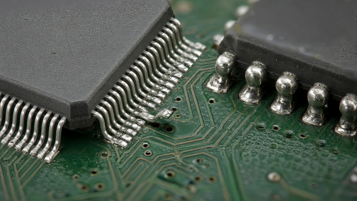
Solder joint opens include non-wetting, head-in-pillow, insufficient paste, lifted leads, and fatigue cracks. Their corrective actions are in stencil design, paste handling, profile, component and board warpage at reflow temperature, and pad finish condition.
What to put in an 8D or RMA request
An 8D is only as good as the problem statement it starts from. We regularly receive requests that say "boards failing, please provide 8D." The result is a generic 8D that lists process controls the factory already has, because there is no specific failure to analyze. The request below is the structure we suggest buyers send—to us or to anyone else.
D1–D2: team and problem description
- Part number, revision, and the files revision the boards were built to.
- Lot, date code, and serial numbers of failed boards; quantity failed out of quantity inspected or deployed.
- Where it was found: incoming inspection, assembly test, system test, burn-in, field.
- The failing net, the two end points, the localization result, and the measured values on failed and good boards.
- The condition under which the open appears: always, hot, cold, flexed, after a number of cycles.
- Photos with the defect location marked.
- Process history: number of reflow and rework passes, coating, thermal cycling, mechanical events.
D3: containment you expect
State what you need: a hold on remaining stock of the same lot, a screen on finished goods at the factory, replacement quantity, or a sort at your site. Ask the factory to state which lots are potentially affected and why—same panel, same plating load, same lamination cycle, same reflow day.
D4: root cause, with the evidence you want to see
Ask for the physical defect location confirmed by analysis, the process step that created it, and why that step's controls did not catch it. Request the microsection images (unetched and etched where relevant), X-ray images, any SEM/EDS data, and the relevant process records: plating log, desmear parameters, electrical test record, reflow profile, rework log. "Operator error" is not a root cause; ask what allowed the error to escape.
D5–D7: corrective and preventive action
Ask for actions that address both occurrence (why the defect was made) and escape (why it was not detected), with a date and the evidence that will show effectiveness—for example, additional coupon cross-sections on the next lots, a thermal stress test on coupons, or a changed test program. Preventive actions should state which other part numbers share the same process risk.
D8: closure criteria
Agree in writing what closes the case: a number of lots without recurrence, coupon results within limits, or a successful requalification build.
Cost traps in open-circuit claims
Several patterns repeatedly inflate the cost of an open-circuit investigation without improving the answer.
- Sending only the failed board. Without a passing reference, many observations cannot be judged.
- Rework before analysis. Once a joint is reflowed, its original microstructure is gone.
- Requesting everything. Ordering SEM, EDS, dye-and-pry, and sectioning on every board in parallel is slow and can destroy the evidence one method needs for another. Sequence from non-destructive to destructive.
- Letting fab and assembly suppliers argue. If fab and assembly are separate vendors, agree up front who analyzes what, and send the same evidence pack to both. With fab and PCBA in one factory, the internal records can be joined directly, which is one practical reason buyers consolidate.
- Undefined thermal history. "It failed in the field" without cycle count, temperature range, or rework count makes it impossible to separate a latent defect from an end-of-life wear-out.
Design and RFQ choices that reduce future opens
Investigations should feed back into your documentation. The most common upstream fixes we see:
- Specify the performance class and plating requirements on the fab drawing, and request coupons or microsection reports for builds where reliability matters.
- Choose laminate for the thermal history the board will actually see, including rework passes, not just the first reflow.
- Review aspect ratio of thick boards with small vias; a modest via diameter increase can reduce barrel stress.
- Protect BGA corners from depaneling and handling flexure, and keep connectors that see insertion force away from area arrays or support them mechanically.
- Add test access to nets that are hard to localize. A few test points on critical power and clock nets dramatically shorten future localization.
- Lock the file set: netlist, drawing, stack, and assembly files that match the build, so bare-board test compares against the right netlist. Our Manufacturing Files guide lists what belongs in that set.
How we handle open-circuit returns at XFPCB
When a customer sends us an open-circuit return, we start with the evidence pack described above. We check the bare-board electrical test record for that lot and serial range, review the assembly records for the board, and then localize electrically on the returned board before anything destructive happens. We confirm the location with X-ray where joints are involved and section the identified feature together with a reference feature. The report states what was found, where, which process step is responsible, and what we will change, and we share the images rather than only conclusions. If the evidence points away from our processes—for example, to field mechanical damage or to a component—we say so and show why, because an honest root cause is the only one that prevents the next failure.
If you are preparing a return or want a second opinion on an open-circuit failure, send us the localization data and photos first. Often a short review of where the open sits is enough to decide which analysis is worth paying for, and which questions your 8D request should ask.