
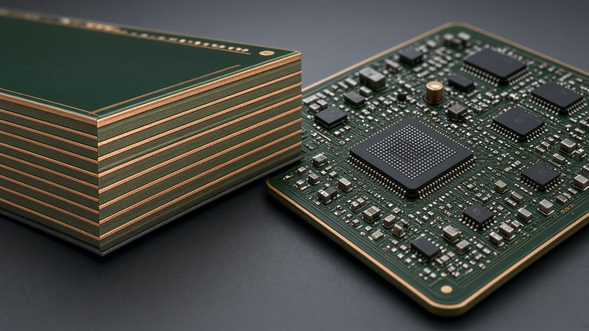
Most stack-up articles list a few textbook layer orders—signal, ground, power, signal for four layers; a couple of options for six—and stop. Those orders are reasonable defaults, but they are answers without the question. The real engineering work in stack design is deciding which layers your particular board needs, what each layer does, which plane each signal layer refers to, and how the stack stays mechanically balanced. That work looks different for an industrial controller, an automotive module, a server board, and a power converter, because the dominant risk in each is different.
This article is about the engineering of stack design: a method for assigning layers, the rules that keep it sound, and how the method changes by application. It is deliberately not about how to document a stack-up so that the fab builds it exactly—that is covered in our post on the stack-up as a fab document. Here the question is what the stack should be before anyone writes it down. We write from XFPCB's CAM and lamination side, where we review hundreds of proposed stacks a month and see which design decisions survive fabrication and which create problems later.
Start from the dominant risk, not from a layer count
A stack is a compromise between signal integrity, power integrity, EMC, thermal behavior, manufacturability, and cost. On any given board, one or two of those dominate. Naming them first makes the rest of the decisions easier.
- Signal integrity dominant: high-speed serial links, memory interfaces, RF. The stack must give controlled impedance, solid unbroken reference planes, and low-loss paths.
- Power integrity dominant: processors and FPGAs with many rails and high transient current. The stack must give low-inductance power delivery, closely coupled power–ground plane pairs, and room for decoupling.
- EMC dominant: products with long cables, metal enclosures with apertures, or strict emissions limits. The stack must contain fields, keep return paths short, and shield outer layers where possible.
- Thermal or current dominant: power stages, motor drives, LED drivers. The stack must carry current and spread heat, often with heavy copper and thick dielectrics.
- Cost or density dominant: consumer products. The stack must achieve routing with as few layers and as standard a construction as possible.
Once the dominant risk is clear, the layer count follows from routing demand and that risk, not the other way round.
A layer assignment method
The method we use when reviewing or proposing a stack runs in a fixed order.
1. Estimate routing layers
Routing demand comes mainly from the densest part—usually the BGA escape. The number of signal rows that must escape under a fine-pitch array, the via technology available, and the trace/space you can afford together determine how many signal layers that escape needs. Add layers for buses that must be routed with impedance control and for any keep-out-heavy areas. This gives a minimum count of signal layers.
2. Give every signal layer a reference plane
Each signal layer needs an adjacent, continuous reference plane—normally ground. A signal layer without an adjacent plane has poorly defined impedance and a return path that wanders, increasing crosstalk and emissions. Two signal layers between the same pair of planes (a "dual stripline") are acceptable if routed orthogonally and spaced to limit broadside coupling, but each is then less tightly referenced.
3. Decide the plane structure
Count the ground planes needed to reference all signal layers, and the power planes needed to deliver your rails. Where possible, place power and ground planes adjacent with a thin dielectric between them; that pair provides distributed capacitance and low inductance. Split power planes carry several rails but create gaps that signals on adjacent layers must not cross.
4. Place high-speed and sensitive layers
Put the most critical signals on inner stripline layers between two ground planes, where they are shielded and their impedance is stable. Outer layers suit component escape, short connections, and microstrip routing where lower dielectric loss or easy rework is wanted.
5. Check symmetry and balance
The stack should be symmetrical about its center in dielectric thickness, material type, and copper weight, and copper distribution on mirrored layers should be similar. Asymmetry causes bow and twist through lamination and reflow.
6. Check manufacturability
Confirm with the fabricator that dielectric thicknesses are buildable with available prepreg and core, that copper weights suit the trace and space, that aspect ratios for the drilled vias are within capability, and that any sequential lamination for microvias or buried vias is necessary and specified.
7. Iterate on cost
If the layer count is higher than expected, look for routing improvements first (escape strategy, via technology, part placement) before accepting an unreferenced layer or a compromised plane.
Rules that hold across applications
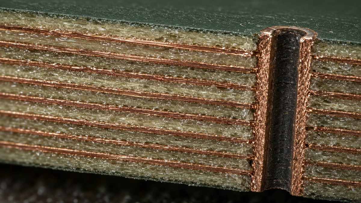
No signal layer without a reference. This is the most violated rule in stacks we review. A six-layer board with signal layers on 1, 2, 5 and 6 and planes only on 3 and 4 leaves layers 2 and 5 referencing planes across thick dielectrics or each other.
Don't route across plane gaps. A signal crossing a split in its reference plane loses its return path; the return current detours around the split, creating a loop that radiates and couples. Either keep splits away from signal routes or stitch with capacitors where crossing is unavoidable.
Layer transitions need return vias. When a high-speed signal changes layers, its return current must also change reference planes. Place ground vias next to signal vias when the reference changes from one ground plane to another; if the reference changes from ground to power, the return path goes through decoupling capacitance, which is less predictable.
Keep power–ground pairs close. A thin dielectric between power and ground increases plane capacitance and reduces loop inductance. Thick separation wastes the plane pair's benefit.
Balance copper. Large copper pours on one side and sparse routing on the other create both warpage and uneven plating. Use balanced fills where electrically harmless.
Choose materials consistently. Mixing laminate systems is sometimes necessary (low-loss for RF layers, standard FR-4 elsewhere), but every mix adds lamination and CTE considerations. Do it on purpose.
How the stack changes by application
Industrial control and instrumentation
Industrial controllers often combine moderate-speed digital logic, analog measurement, isolated interfaces, and field wiring. The dominant risks are usually EMC immunity and mixed-signal noise, plus creepage around isolation barriers.
Stack considerations:
- A four- or six-layer stack with at least one continuous ground plane under the digital and analog sections.
- Analog and digital ground handled on one plane with partitioned placement, rather than separate split planes that signals then cross.
- Isolation barriers carried through all layers: no copper of either side crossing the barrier on any layer, with the barrier width set by the creepage and clearance requirement.
- Thicker outer copper sometimes needed for relay and terminal currents.
Our Industrial Control work frequently involves exactly these isolation-driven stacks.
Automotive electronics
Automotive modules face thermal cycling, vibration, and strict EMC requirements, with long harnesses acting as antennas.
Stack considerations:
- Ground planes adjacent to outer routing layers to contain fields, and sometimes ground on both outer layers with signals buried.
- Material selected for thermal cycling and CAF resistance, with a Tg and expansion behavior appropriate for the mission profile.
- Symmetric construction to keep boards flat through multiple reflows and under-hood temperature swings.
- Careful via design and plating requirements, since barrel fatigue under thermal cycling is a primary failure mode.
See Automobile Electronics for the types of boards we build in this sector.
Server, storage, and high-speed communication
These boards carry many high-speed serial lanes and wide memory buses, with large BGAs and high power processors.
Stack considerations:
- High layer counts driven by BGA escape and lane count, often with many stripline layers each between two ground planes.
- Low-loss materials on high-speed layers, with glass style and copper roughness chosen for the loss budget.
- Multiple power–ground plane pairs close to the processor for low-impedance power delivery.
- Back-drilling or blind vias to reduce via stubs on high-speed lanes.
- Strict control of dielectric thickness and impedance, with fabricator-confirmed constructions.
Our Server & Data Storage boards typically fall in this category.
Power conversion and motor drives
Power boards are dominated by current, heat, and high voltage, with fast-switching nodes that generate noise.
Stack considerations:
- Heavy copper on power layers, which constrains minimum trace and space on those layers and affects lamination resin fill.
- Thicker dielectrics where high voltage between layers requires it, chosen against insulation requirements.
- A solid ground plane close to the switching loop, so that the high di/dt loop area is small.
- Gate-drive and control circuitry referenced to a quiet plane, separated from power copper by layer assignment rather than by distance alone.
- Thermal vias and copper planes used as heat spreaders, with symmetry maintained despite heavy copper on some layers.
Consumer and compact devices
Consumer boards are dominated by cost and density, often with fine-pitch packages and RF radios in small enclosures.
Stack considerations:
- The fewest layers that achieve routing with adequate reference planes, often four to eight.
- HDI microvia structures where they reduce layer count enough to pay for themselves.
- RF sections with a dedicated ground reference and controlled impedance on the antenna feed, often on the outer layer with ground immediately below.
- Thin overall thickness, which increases warpage risk and makes symmetry more important.
A worked example: eight layers, two ways
Consider a board with a fine-pitch processor, a memory interface, a few high-speed serial lanes, and four supply rails. Routing estimation says four signal layers are needed.
A tempting arrangement is signal–ground–signal–signal–power–signal–ground–signal. It provides four inner routing layers, but layers 3 and 4 sit next to each other between ground and power, coupling broadside, and layer 6 references a split power plane. The memory interface and serial lanes have nowhere quiet to go.
A sounder arrangement is signal–ground–signal–power–ground–signal–ground–signal. Layers 3 and 6 are striplines between solid references, suited to the serial lanes and memory. Layers 4 and 5 form a closely coupled power–ground pair near the center for power delivery. Outer layers handle escape and short routes over ground. The construction is symmetric about the center pair. It gives up one inner routing layer compared with the first option, so escape routing and via strategy have to be planned to fit—but every signal layer now has a defined reference, and the board is easier to build flat.
The point is not that one order is always right; it is that each layer's job and reference are decided deliberately.
Common stack design mistakes we see
- Six layers with two unreferenced signal layers, chosen to "get more routing" without understanding the reference penalty.
- Split power planes under high-speed routes, causing return-path discontinuities.
- Asymmetric stacks with thick prepreg on one side and thin on the other to hit an impedance target, producing warped boards.
- Heavy copper on one outer layer only, creating both warpage and plating imbalance.
- Dielectric thicknesses that no available prepreg combination produces, forcing a redesign after quote.
- Impedance targets calculated with the wrong Dk for the actual construction.
- Too many lamination cycles from mixing blind, buried, and microvia structures where a simpler via scheme would work.
When to involve the fabricator
The best time to involve the fabricator in stack design is after you have a candidate layer assignment and before layout begins. At that point we can confirm that dielectric thicknesses are buildable, propose constructions with known materials, calculate trace geometries for impedance targets with construction-specific Dk, and flag via structures that add cost. Our 6-Layer PCB page shows the types of constructions we commonly build at that layer count.
Changing the stack after layout is expensive because trace widths, via structures, and sometimes routing must change. Changing it before layout costs an email.
Before layout starts: the stack sign-off
The stack is ready to hand to layout when you can answer each of these for your own board, in writing:
| Question | Acceptable answer looks like |
|---|---|
| What is the dominant risk? | One or two named: SI, PI, EMC, thermal/current, cost |
| What does each layer do? | Signal, ground, or power, with the nets or interfaces it carries |
| What does each signal layer reference? | A named, continuous plane directly adjacent |
| Where are the plane splits? | Listed, with no critical route crossing them |
| Where do high-speed signals change layers? | Return-via plan beside each transition |
| Is the stack symmetric? | Dielectric, material, and copper mirrored about the center |
| Is it buildable? | Dielectric thicknesses and impedance widths confirmed by the fabricator |
| What did you give up? | The routing or cost trade you accepted, stated plainly |
If any row is blank, the layout will answer it for you—usually in the least convenient way. Once every row is filled, freeze the construction and move on to documenting it.