

When an assembled board comes back with an open circuit, the first question is usually whose problem it is. Was the break in the bare board, or did it happen when parts were soldered on? The answer decides who investigates, what changes, and whether the rest of the lot is at risk. It's also less obvious than it looks, because some fabrication defects pass every bare-board test and only open once the board has been through reflow.
This article walks through where opens start in fabrication and in assembly, the signature each type tends to leave, and which inspection or test stage is in a position to catch it.
Opens that start in fabrication
Our PCB Fabrication Process page lays out the sequence from imaging and etching through lamination, drilling and plating. Each of those steps has its own way of producing an open.
Imaging and etching. A particle on the phototool or dry film, a scratch in the resist, or a local over-etch can cut a trace or neck it down to a sliver. On inner layers, these are looked for with optical inspection before lamination, because once the layer is buried the only way to see it again is to cut the board. Signature: a clean gap or severe neck in the copper, located at the same place on one board but not repeating across boards (a repeating location points to the phototool or the data instead).
Drilling and registration. If a hole lands off-centre on an inner-layer pad, the annular ring can break out. When the breakout is where the trace joins the pad, the connection is reduced or lost. Signature: seen in a microsection as a hole cutting through the pad edge at the trace junction.
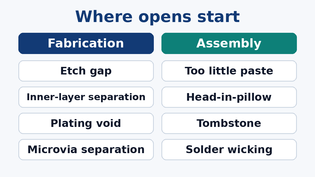
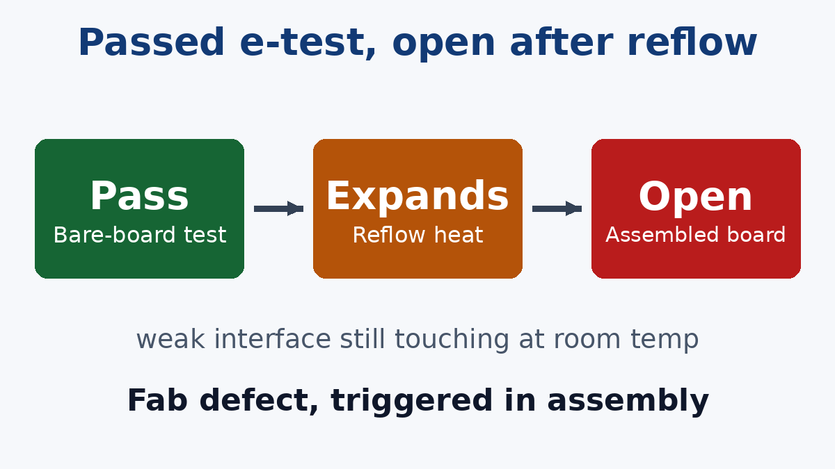
Desmear and electroless copper. Drilling leaves resin smear on the exposed inner-layer copper inside the hole. If desmear doesn't remove it, or the electroless copper doesn't bond well to the inner-layer copper, the joint between the inner layer and the plated barrel is weak. This is usually called an interconnect defect (ICD), or inner-layer separation. It's one of the most important fabrication opens to understand because the interface can still be touching at room temperature. Bare-board electrical test passes. Then the board expands through its thickness during reflow, the weak interface separates, and an open or an intermittent connection appears after assembly.
Plating voids and thin barrels. Air trapped in a hole, poor solution exchange in small or deep holes, or debris can leave voids in the copper plating. A severe void opens the barrel completely. A partial one may conduct at test and crack later.
Barrel and corner cracks. In thick boards and in materials with high expansion through the thickness, repeated heating strains the plated barrel. Cracks tend to start at the knee of the hole or mid-barrel. They often show as opens that come and go with temperature.
Microvia separation. On boards with laser-drilled microvias, the base of the microvia can separate from the target pad beneath it, often linked to residue left after laser drilling or a weak electroless layer. Like ICDs, these can pass at room temperature and open after reflow, sometimes reconnecting when hot and opening again when cool. Stacked microvia structures on HDI PCB builds are the usual place this comes up.
Opens that start in assembly
Not enough solder. A clogged stencil aperture, poor paste release or a smeared print leaves too little paste on a pad. The joint never forms, or forms as a thin fillet that cracks. Solder paste inspection (SPI) before placement is the stage that sees this most directly.
Lifted leads and coplanarity. A bent lead on a gull-wing package, or a part that isn't flat, can leave one lead sitting above its paste. Signature: the joint shows no wetting on the lead, often with a good fillet on the pad.
Head-in-pillow. On BGAs, the board or the package can warp during reflow so that a ball lifts off its paste deposit, then settles back after the paste has started to solidify. The ball and the paste sit together without merging into one joint. Electrically it may make contact and pass test, then open under handling or temperature. It's hard to see, which makes it one of the more troublesome assembly opens.
Non-wet opens. The opposite case: paste stays on the pad and the ball separates from it entirely, usually because of warpage or contamination.
Tombstoning. Small two-terminal parts stand up on one end when the two joints wet at different times, leaving one end open. Usually visible to post-reflow optical inspection.
Solder wicking. Solder can run up a lead or drain into an unfilled via inside a pad, starving the joint. Via-in-pad designs normally call for filled and capped vias for this reason, which makes it a fabrication specification issue that shows up in assembly.
QFN and thermal pad float. Too much paste on a large centre pad can lift the package so the perimeter terminations don't wet properly.
Mechanical damage. Board flexing during depaneling, fixture testing or connector insertion can crack joints, crack ceramic capacitors internally, or fracture the laminate under a BGA pad (pad cratering), taking the trace connection with it.
Some opens sit on the boundary
A few causes don't belong cleanly to either side:
- Surface finish problems. A defective nickel layer under an immersion gold finish, for example, can give joints that fracture at the interface. The symptom appears in assembly but the root cause is in fabrication.
- Latent fabrication defects triggered by assembly heat. ICDs, weak microvias and marginal barrels are fabrication defects, but assembly reflow is what opens them. A board that passed bare-board test and failed after reflow hasn't automatically been damaged by the assembler.
- Design and specification. A missing via in the data, unfilled via-in-pad, or a thin thermal relief that cracks under handling is neither a fabrication nor an assembly process failure.
Reading the signature
When opens are found, a few questions narrow the cause before anyone cuts a board:
| Question | Points toward |
|---|---|
| Is the break inside the board, or at a solder joint? | Inside: fabrication or design. At the joint: assembly or finish |
| Did the bare board pass electrical test? | Passing doesn't rule out ICDs, microvia separation or marginal barrels |
| Does the fault change with temperature or flexing? | Cracked barrels, microvia separation, head-in-pillow, cracked joints |
| Is it the same location on many boards? | Design, data, phototool or a systematic process issue |
| Random locations across the lot? | Process variation: paste printing, plating, handling |
| Only on boards from one panel or one date? | A specific lot or process window |
For fabrication suspects, a cross-section through the failing hole or microvia identifies which interface separated. For hidden assembly joints, X-Ray Inspection of BGA and QFN joints is usually the first non-destructive step, followed by cross-section or dye-and-pry if the image isn't conclusive. For suspected latent fabrication defects, bare boards from the same lot can be put through simulated reflow cycles and retested, or coupons from the panel can be sectioned after thermal stress.
Which check catches what
- Inner-layer optical inspection: etching and imaging opens before lamination.
- Bare-board electrical test: opens that exist at room temperature. Not designed to see weak interfaces that are still in contact, or one open path among several parallel ones.
- Microsection and thermal stress of coupons: ICDs, plating voids, barrel quality and microvia interfaces.
- SPI: insufficient or misplaced paste before parts are placed.
- Post-reflow optical inspection: tombstones, lifted leads, visible non-wetting.
- X-ray: hidden joints under BGAs and QFNs, voids, some head-in-pillow cases.
- In-circuit or flying probe test: opens at joints on nets with test access.
- Functional test: opens that stop a function, but without saying where they are.
No single stage catches every type. The useful part of knowing the root causes is choosing which checks a particular board needs, and knowing where to look first when an open turns up.