

Prepreg is the layer of a multilayer board that designers think about least and that changes the most during manufacturing. A core arrives from the laminate supplier at a fixed thickness and stays that way. Prepreg arrives as glass cloth carrying partly cured resin, and during pressing that resin melts, flows into the gaps between copper features, and squeezes out at the panel edges before it cures. What ends up between two layers is not the thickness printed on the prepreg datasheet.
This matters because the dielectric thickness between a trace and its reference plane sets impedance, crosstalk and, for high-voltage boards, insulation. This article is written for the designer or engineer who has to put a stackup on a drawing. It covers how pressed thickness is worked out, how resin content changes the electrical properties, and which prepreg decisions you should make yourself versus leave to the factory.
Nominal thickness and pressed thickness
Prepreg is sold by glass style (common designations include 106, 1080, 2113, 2116 and 7628, from thin and fine to thick and coarse) and by resin content. Each combination has a nominal thickness, usually quoted for pressing between plain surfaces with no copper pattern to fill.
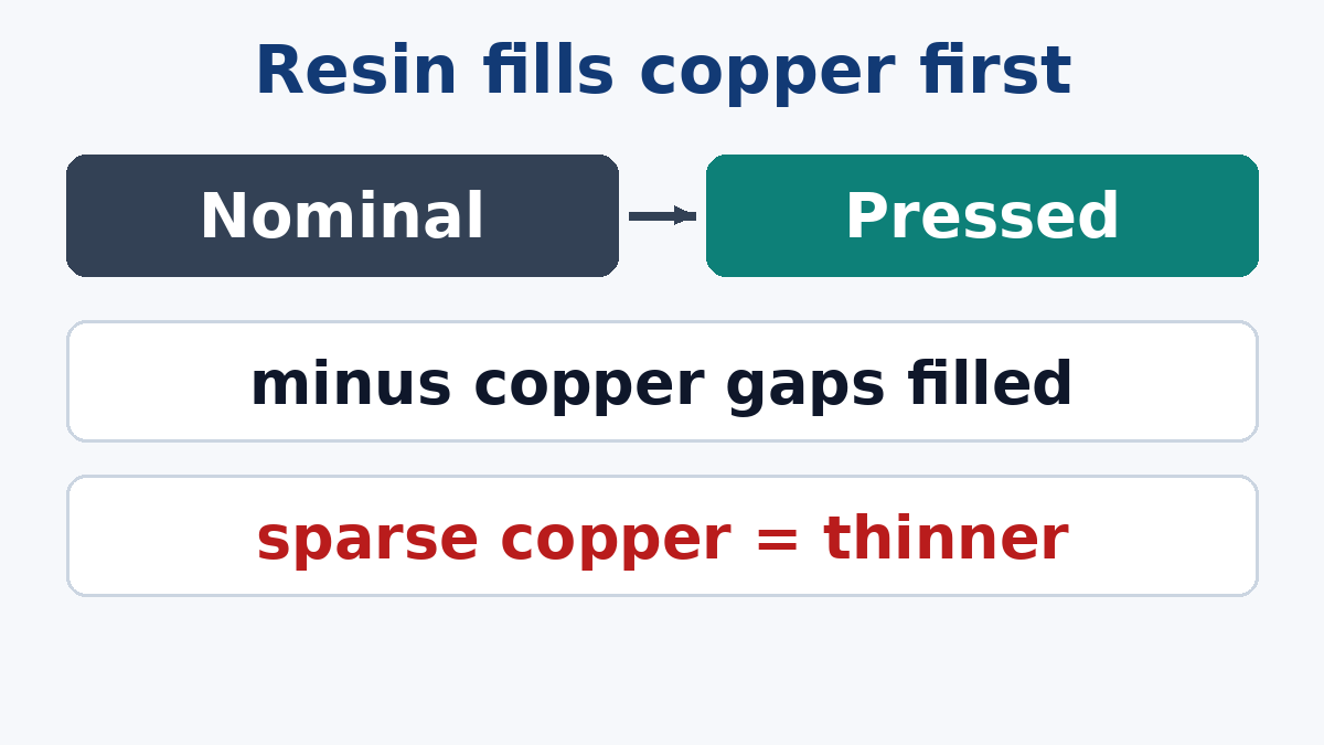
On a real board, the resin also has to fill the spaces where copper was etched away on the adjacent inner layers. That resin comes out of the prepreg's thickness. A simple estimate used across the industry is:
pressed thickness ≈ nominal thickness − Σ (1 − copper coverage) × copper thickness
where the sum runs over each adjacent inner-layer copper surface that the prepreg must fill, and copper coverage is the fraction of that layer's area that remains copper.
An illustration of the arithmetic: a prepreg ply with a nominal 100 µm, facing one inner layer of 35 µm copper with 30% coverage, loses about 0.7 × 35 ≈ 25 µm to fill and presses to roughly 75 µm. The same ply facing a solid plane loses almost nothing. Two signal layers with sparse copper on either side lose fill to both.
Factories use their own pressed-thickness data, measured from microsections of their materials and press cycles, rather than this simple formula. But the formula explains why the same prepreg gives different thicknesses in different places on the same stackup.
Resin content: more than glue
Within one glass style, prepreg is usually offered in several resin contents. Higher resin content gives more resin to fill copper, a thicker pressed result for the same glass, and more flow. It also changes the electrical properties: resin has a lower dielectric constant than glass, so higher resin content means lower Dk, and resin content affects loss too.
That has two practical consequences:
- Dk is not a single number for a material family. The Dk the factory uses for impedance calculation depends on the glass style and resin content in each dielectric layer. If you calculate impedance with one generic Dk for "FR-4", expect the factory's stackup to come back with adjusted line widths.
- Too little resin is a reliability risk. Low-resin prepreg facing heavy or sparse copper can leave unfilled areas. Lamination voids and resin starvation are covered in our separate article on voids and delamination; for stackup planning, the point is that resin needed for fill is part of the prepreg choice, not an afterthought.
Glass style and what it does to signals
Coarse glass styles have large gaps between fibre bundles, filled with resin. A narrow trace running along a bundle sees a higher Dk than one running over a resin-rich gap. For a differential pair, that can create skew between the two lines. Finer and spread-glass styles, where the bundles are flattened to fill gaps more evenly, reduce this effect.
For most boards, glass style is not a concern. For high-speed differential links, especially long ones, specifying a spread-glass or fine-weave style for the signal layers, or routing at a slight angle to the weave, is a known mitigation.
Plies: one, two or more
A dielectric layer can be built from one ply of prepreg or from several. Several plies give more freedom to hit a target thickness and more resin for fill. Some high-reliability drawings require at least two plies between conductive layers, on the reasoning that a defect in one ply is unlikely to line up with a defect in the next. If your product or customer has such a requirement, state it; otherwise the factory will choose what gives the thickness and fill.
Very thin single-ply dielectrics are also where insulation and CAF concerns concentrate. For boards with significant voltage between adjacent layers, check the dielectric thickness after pressing, not the nominal.
What to lock and what to leave to the fab
The most common stackup problem we see is over-specification in one place and under-specification in another: a drawing that names the exact prepreg style for every layer but gives no impedance targets, or one that gives impedance targets but a total thickness that cannot be met with available materials.
A practical division of responsibility:
Specify yourself:
- Layer count, copper weights and finished board thickness with tolerance
- Material family and required properties (or an IPC-4101 specification sheet)
- Impedance targets with tolerances, and the layers and reference planes they apply to
- Any minimum dielectric thickness for insulation, or minimum ply count if required
- Glass style for specific layers only where you have a reason (skew-sensitive links, a qualified stackup)
Leave to the factory, then approve:
- Exact prepreg styles, resin contents and ply counts
- Final line widths to meet impedance, within limits you set
- Core selection to meet total thickness
Then ask for the factory's proposed stackup, with pressed thicknesses and Dk values per layer, before production. On a controlled-impedance design, this approval step is where most surprises can be caught cheaply. Our Impedance Control PCB process works this way.

Design choices that make prepreg behave
Balance copper. Large empty areas next to dense copper give uneven fill, uneven thickness and more risk of voids. Copper pour or thieving on sparse layers, where the circuit allows, evens it out.
Keep the stackup symmetric. Mirror the dielectric and copper structure about the centre of the board. Asymmetric prepreg and copper distribution contributes to warpage.
Plan for heavy copper. Thick inner copper needs high-resin prepreg, often in more than one ply, and thicker dielectric to fill it. If your design has heavy inner layers, involve the fab before fixing the dielectric thickness. See our Heavy Copper PCB page for the build considerations.
Avoid stacking all tight requirements on one layer. A very thin dielectric, a tight impedance tolerance and heavy copper on the same layer pair is the hardest combination to build consistently.
A stackup note that works
A useful stackup note looks something like this: 8 layers, 1.6 mm ±10% finished, inner copper as listed, material per IPC-4101 with Tg and Td requirements stated, impedance targets per the table, fabricator to select prepreg styles and submit stackup with pressed thicknesses and Dk for approval before production. If you have a reason to fix glass style on certain layers, add it as a separate line with the reason.
If you would like a stackup proposal for a new design, send us the layer count, copper weights, thickness and impedance requirements. Our engineers will return a stackup with the prepreg choices and pressed thicknesses we would build, so you can check it against your design before layout is finished.