
A single-sided flex circuit is one copper layer on a flexible base film, protected by a coverlay. IPC-6013, the performance specification for flexible boards, calls it Type 1. It is the simplest flex construction and usually the cheapest, and it covers a large share of real flex applications: display and sensor tails, battery connections, simple jumpers between boards, LED strips, keypads.
Simple does not mean free of design decisions. Having only one copper layer changes several things that designers used to rigid boards or multilayer flex tend to overlook. There are no plated holes to anchor pads, no second layer for crossovers or a ground plane, and the copper's position in the thickness of the circuit decides how well it survives bending. This article covers those single-layer specifics. Materials, bend radius rules and connector tails have their own articles; here we focus on what is different when there is only one layer.
The construction
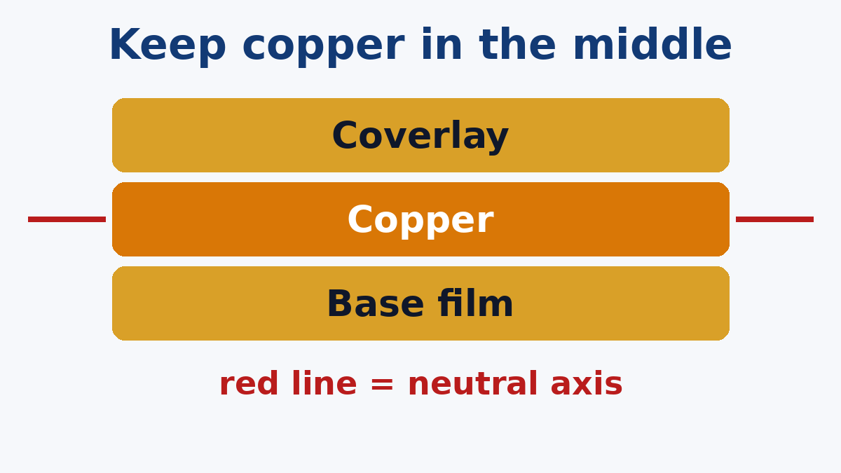
From one side to the other, a typical single-sided flex circuit is: base film (usually polyimide), adhesive (or an adhesiveless bond), copper, coverlay adhesive, coverlay film. Stiffeners are added locally under connectors and components. Openings in the coverlay expose pads; the copper can also be exposed from the base side in "dual access" constructions, which we cover separately.
The flex design standard IPC-2223 covers the design rules for all of this, including single-sided circuits.
Put the copper on the neutral axis
When a strip of material bends, the outer surface stretches and the inner surface compresses. Somewhere in between is a plane that does neither: the neutral axis. Copper placed on or near that plane sees the least strain when the circuit bends. Copper far from it sees the most, and that is where fatigue cracks start.
A single-sided circuit has a big advantage here. With only one copper layer, you can place it on the neutral axis by making the construction roughly symmetric: the coverlay film and adhesive on one side about the same thickness as the base film and adhesive on the other. Then the copper sits in the middle.
The common mistake is to choose a thin coverlay over a thicker base, or to add a thick coverlay for protection without considering bending. That moves the neutral axis away from the copper. For a static install bend it may not matter. For a circuit that flexes in use, it shortens life.
For dynamic applications, combine this with rolled-annealed copper, traces running perpendicular to the bend line, no pads or openings in the bend area, and the largest bend radius the product allows.
Anchor the pads
On a rigid board or a double-sided flex, a pad with a plated hole is held to the board by the plated barrel. On a single-sided flex, a surface-mount or solder pad is held only by the adhesive bond between the copper and the base film. Heat from soldering softens adhesives, and mechanical stress from flexing near the pad, cable pull or rework can peel it away.
The standard ways to make pads more robust:
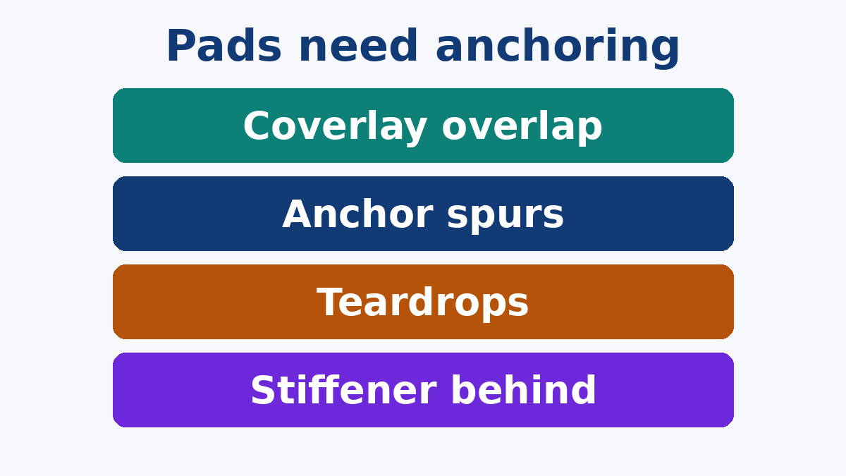
- Coverlay-defined pads. Make the copper pad larger than the coverlay opening, so the coverlay overlaps and holds the pad edges down.
- Anchoring spurs or tie-downs. Small copper extensions from the pad that run under the coverlay, giving it more grip.
- Generous trace-to-pad transitions. Teardrops or tapered entries reduce stress concentration where the trace meets the pad.
- Stiffeners under components. A stiffener on the opposite side of the circuit stops the flex from bending at the solder joints.
For through-hole parts on a single-sided flex, the hole is unplated, and the pad must be anchored the same way. A stiffener with matching holes behind the pad area is common.
Terminations
A single-layer circuit connects to the rest of the product in a few common ways:
- ZIF or FFC connector tail. Exposed contacts at the end of the circuit, with a stiffener to bring the tail up to the connector's thickness specification. The total thickness tolerance at the contacts matters more than anywhere else on the circuit.
- Soldered to a rigid board. By hand, hot bar or reflow, often with pads on the end of the circuit. The stiffener and pad anchoring rules above apply.
- Crimped contacts. Common for LED strips and some sensors.
- Anisotropic conductive film. For fine-pitch connections to displays and glass.
Decide the termination early. It determines the stiffener, surface finish and thickness requirements at the end of the circuit.
When one layer is not enough
The single-sided construction runs out in a few predictable ways:
Crossovers. Every net must be routed without crossing another. Simple circuits manage this; anything with a bus or a matrix soon needs jumpers or a second layer.
A reference plane. Controlled impedance and good EMI behaviour usually need a ground plane next to the signal traces. On a single layer, the only option is coplanar routing with ground traces alongside the signals, which works for some cases but uses width. If you need a real plane, you need a second layer or a shielding film.
Current. Thin copper on a single layer limits current per trace width. Wider traces solve it until the circuit becomes too wide.
Density. Fine pitch parts with many pins rarely fan out on one layer.
When one of these hits, the options are a double-sided flex, a shielding film on a single-sided circuit, or moving part of the circuit onto a rigid board. Our Flexible PCB Capability page lists the constructions we build if you are weighing the step up.
What affects cost on a single-sided flex
- Outline and nesting. Flex material is expensive and the circuit outline determines how many fit on a panel. L-shapes and long tails use material poorly; sometimes a folded design nests better.
- Coverlay openings. Many small openings, especially close to each other, take more work and need tighter registration than a few large ones.
- Stiffeners. Each stiffener type and thickness adds a part and a bonding step.
- Copper and film thickness. Standard thicknesses of base film and copper are cheaper and easier to source than unusual ones.
- Tolerance. Tight outline tolerances need more precise cutting; ask which are really needed.
A checklist before you release a single-sided flex
- Coverlay and base thickness balanced if the circuit flexes in use
- Copper type (RA or ED) suited to the bend requirement
- Pads anchored by coverlay overlap or spurs, teardrops on trace entries
- No pads, openings or stiffener edges in the bend area
- Stiffeners defined with material, thickness and location
- Termination method and thickness tolerance at contacts specified
- Static or dynamic use and bend radius stated on the drawing
If you have a single-sided flex design ready, send us the drawing and a description of how it bends in use. Our engineers will check the construction balance, pad anchoring and terminations before you commit to tooling.