
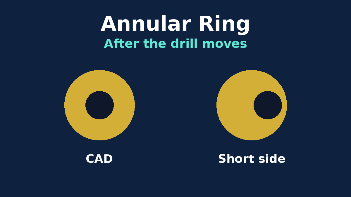
The annular ring in a CAD tool is a drawing. The annular ring on a finished board is whatever copper is still there after the hole is drilled off-center, the wall is plated, and the inner layers have moved a little relative to that drill. Buyers who argue from the CAD number, and factories who accept or reject from the finished board, are often measuring two different things.
The number in CAD is the centered case
For a round pad and a round hole, the nominal ring is half the difference of the diameters:
(pad − hole) / 2
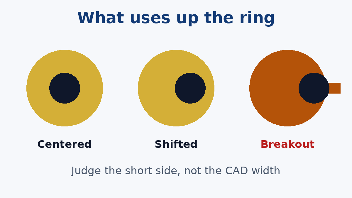
The mistake that still shows up on drawings is to treat the full difference as the ring. A 0.60 mm pad and a 0.30 mm hole differ by 0.30 mm across the hole. The ring on one side is 0.15 mm. That figure also assumes the hole is perfectly centered. Manufacturing never is, so the number that matters is the short side, not the average.
Which hole you subtract matters just as much. The finished hole is the opening after plating. The drill that cut the glass was larger, because the plated wall takes space. As an illustration only, 25 µm of copper on the wall means a 0.30 mm finished hole was drilled at about 0.35 mm. On a 0.55 mm pad the external picture, measured to the finished hole, is (0.55 − 0.30) / 2 = 0.125 mm. The internal picture, measured to the drill, is (0.55 − 0.35) / 2 = 0.10 mm, and that is before the inner layer shifts at all. None of those thicknesses is a factory specification. They are there to show why a pad that looks generous against the finished hole can be tight against the drill.
Drill, then plate, is the order described on our PCB Fabrication Process page. That order is the whole reason the drill and the finished hole are not interchangeable in the ring calculation.
External and internal rings are not the same measurement
IPC-6012 does not measure the ring the same way on the outside of the board as it does on an inner layer.
On an external layer the ring is the copper between the edge of the plated hole and the edge of the land. Plating has already narrowed the hole, so this measurement gives some of the drill's extra diameter back.
On an internal layer the ring is the copper between the edge of the drilled hole and the edge of the land. The inner pad never sees the plated wall as a smaller hole. It sees the drill. Layer-to-layer registration then moves that pad relative to the drill, and the short side gets shorter again.
A board can photograph well from the outside and still be thin, or broken out, on an inner layer. The outer land is imaged on the finished panel and tends to follow the drill more closely. Inner lands were etched on separate cores, then pressed, then drilled. Each of those steps spends a bit of the ring.
Continuing the illustration: start from the 0.10 mm internal ring above, and shift that inner layer by 0.08 mm. The short side is 0.02 mm. That is under the 0.025 mm internal minimum associated with Class 3, while the outer layer can still look comfortable. Again, 0.08 mm is not a claim about any shop's registration. It is a reminder that the inner number, not the CAD external number, is the one that fails first. On higher layer counts that stack of cores is longer, which is the practical reason our High Layer Count PCB work, from about ten layers upward, treats registration as part of the build and not as a layout footnote.
What Class 2 and Class 3 actually allow
There is no single minimum ring that every board must meet. IPC-6012, read with the visual criteria in IPC-A-600, sets acceptance by class. The figures below are the ones buyers and CAM engineers usually mean. A drawing that names a different minimum replaces them.
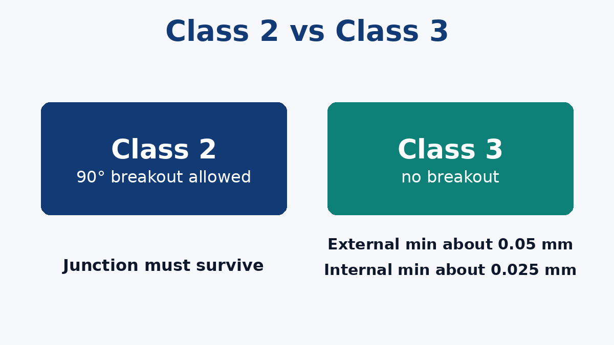
Class 2 allows breakout. Up to 90° of the hole may leave the land, provided the conductor-to-land junction is not cut by more than 20% of the minimum conductor width on the drawing, the junction does not go below 0.05 mm or that minimum width (whichever is smaller), and spacing to other copper still holds. Tangency, where the hole just kisses the pad edge, is inside that allowance.
Class 3 does not allow breakout. The usual minimums are 0.05 mm on external layers and 0.025 mm on internal layers, with a limited reduction of the external minimum where a pit, nick or dent is isolated. A design drawn so that a centered hole has exactly 0.025 mm of internal ring will not meet Class 3 once the drill wanders.
Class 1 is looser still, out to about 180° of breakout, with its own limit on how much the conductor junction may be reduced. Most product drawings that say nothing are built and judged as Class 2. If you needed Class 3, silence does not get you there.
Calling out "Class 3" and also drawing every via at the Class 2 pad is how boards fail coupons. The class on the drawing and the pad in the Gerber have to describe the same board.
Tangency, breakout, and the teardrop
The conditions people mix up:
- Reduced ring. The hole is off center, copper remains all the way around, the short side is simply smaller. This can still be acceptable.
- Tangency. The hole reaches the pad edge at a point. Class 2 can accept this. Class 3 does not.
- Breakout. The hole leaves the pad, so part of the circumference has no land. Class 2 accepts it up to 90° if the trace junction survives. Class 3 does not.
A teardrop widens the copper where the trace enters the pad. That helps the junction, which is exactly the place Class 2 measures when breakout points at the trace. It does not put copper back on the opposite side of the pad, and it does not turn a broken-out Class 3 hole into a passing one. If the note says teardrops are not allowed, CAM should not add them to save a marginal pad. If the note is silent, ask before assuming either way.
What a continuity test will not tell you
A ring that has broken out toward the trace can still be electrically continuous, as long as some copper joins the barrel to the track. Bare-board electrical test is looking for opens and shorts against the netlist. It is not measuring annular ring, and it will not fail a via that is mechanically one nick away from an open.
Our Testing & Inspection page covers electrical test alongside visual and other inspection when a build asks for them. Ring width, especially on inner layers, is a microsection question: a coupon, a cut through the hole, and a measurement of the short side on the layers the class cares about. Ask for that when the design is on the Class 3 minimum, on a thick board, or on small vias where the CAD ring was already tight. Do not expect the flying-probe report to stand in for it.
Laser microvias are a different structure. The capture pad and the laser spot are both smaller, the "drill" is not a mechanical tool wandering in a thick stack, and the acceptance numbers above are for mechanically drilled plated holes. Do not copy a through-hole pad rule onto a microvia, or the other way around.
What to put on the fabrication drawing
- The class, or an explicit minimum ring if you need something other than the class default.
- Whether breakout is forbidden even on a Class 2 build. Some products want tangency as the worst case. That has to be written. Class 2 alone does not say it.
- Finished hole and pad as a pair. Changing the finished hole in CAM without changing the pad spends the ring directly.
- Internal pads included. Deleting unused inner pads is a separate decision. Where a pad stays, it needs the internal ring, not the external one.
- Teardrops: allowed, required, or not allowed.
- A coupon or microsection when the short-side ring is the reliability argument, not just the netlist.
The CAD width is the starting budget. Plating, drill size and registration spend it. The class decides how little you are allowed to have left.