

When a multilayer board shows a pocket between layers, the report often just says "delamination". Sometimes that is correct. Often it is not, and the difference matters, because the defects that look similar in a photograph come from different stages of the process and need different fixes.
A lamination void is an area that the resin never filled during pressing. A delamination is a separation between layers that were bonded, usually caused later by heat and moisture. Blisters are localised delaminations that lift the surface. Measling and crazing are separations between glass fibres and resin inside the laminate itself. IPC-A-600, the acceptability standard for printed boards, treats laminate voids and delamination or blistering as separate conditions with their own criteria, for exactly this reason.
This article explains how each forms, how a microsection tells them apart, and which parts of prevention sit with the factory and which with the design and the buyer.

How a multilayer board is laminated
To understand voids, it helps to picture the press. Inner-layer cores, already etched with their circuit patterns, are stacked with sheets of prepreg (glass cloth impregnated with partially cured resin) and copper foil. Under heat, pressure and usually vacuum, the prepreg resin melts, flows into the spaces between the copper features on the inner layers, wets the surfaces and then cures.
Everything depends on that flow. The resin has to fill the etched-away areas between traces and planes, push out the air, and do so before it gels and stops flowing. Anything that leaves too little resin, too little time or too much trapped gas leaves a void.
Lamination voids: causes
Resin starvation. Each prepreg sheet carries a certain amount of resin. Heavy copper on inner layers creates deep gaps that must be filled, and a thin dielectric built from one sheet of low-resin-content prepreg may not have enough resin to fill them and still leave the required thickness. The result is dry areas, typically in large copper-free regions next to dense copper, or between heavy copper features.
Trapped air and volatiles. Air between the sheets has to be removed by vacuum and by resin flow. Moisture absorbed by prepreg or inner layers, and volatiles from the resin, turn into gas at press temperature and can leave voids if they are not driven out before the resin gels.
Resin flow behaviour. Prepreg that has been stored too long or too warm has partially advanced and flows less. The press cycle's heating rate and pressure timing determine how long the resin stays fluid. These are process-control items within the factory.
Low-flow and no-flow materials. Rigid-flex and some hybrid builds use prepregs designed to flow very little, so they do not run into areas where they are not wanted. They are correspondingly less forgiving of copper height differences.
Delamination and blistering: causes
Delamination is a loss of adhesion at an interface that was bonded: between resin and copper, or between prepreg and core. It usually appears when the board is heated, during hot air levelling, reflow, rework or thermal testing.
Moisture. Epoxy-based laminates absorb moisture from the air. During reflow, that moisture turns to vapour and the pressure can separate layers, especially at interfaces that were already weak. A board that has sat for months in an open bag in humid conditions is much more likely to blister in reflow than the same board fresh from the factory.
Weak bonding treatment. Inner-layer copper is treated (oxide or an alternative bonding treatment) to give the resin something to grip. Contamination, an incomplete treatment or handling damage weakens the bond.
Thermal demand beyond the material. Lead-free reflow temperatures, multiple reflow passes and rework push the resin system. Materials differ in decomposition temperature and in time to delamination at high temperature. A standard material that is adequate for a single reflow may not be adequate for a double-sided board with rework on a thick, high-layer-count stackup.
Mechanical and CTE stress. Large differences in expansion between materials, as in hybrid stackups or boards with metal inserts, add stress at interfaces during heating.
Measling and crazing
These occur inside the laminate, at the glass weave: small white spots or connected white areas where the resin has separated from the fibres. They can be caused by thermal or mechanical stress. IPC-A-600 treats them as externally observable conditions with their own criteria; they are often cosmetic, but they can matter where they reduce spacing between conductors, especially on boards that see high voltage or humidity.
Telling them apart
The main diagnostic tool is a microsection, ideally from a defect area and from an area next to it.
- A lamination void is an empty area with smooth resin edges, often with the shape of the gap between copper features, and no sign of fracture. It was never filled. It may be present on boards that have never seen solder.
- Delamination shows a separation along an interface, with fracture surfaces that once were bonded. It is typically found after a thermal event, and it may be absent on unsoldered boards from the same lot.
- A blister is delamination near the surface, visible from outside as a raised area.
- Measling and crazing are within the glass and resin layer, not along an interface.
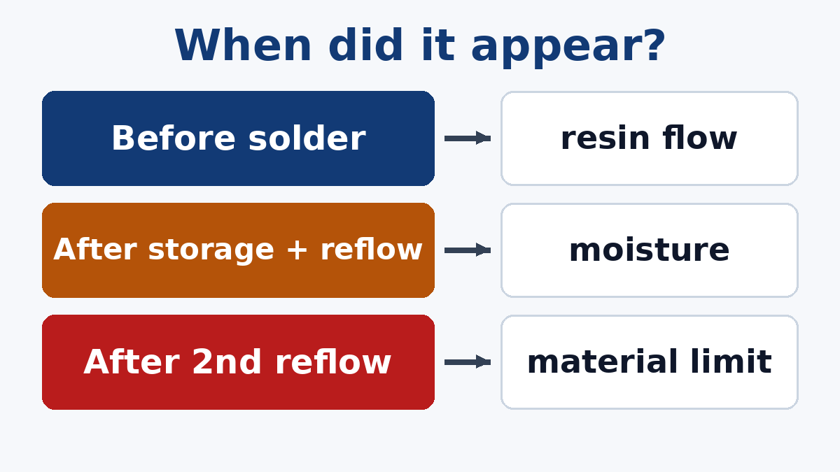
When the defect appeared is often as telling as the section. A defect present at incoming inspection points to the fabrication process. A defect that appears only after reflow, and only on boards that were stored for a long time, points to moisture. A defect that appears on every board after the second reflow pass points to the material's thermal capability.
IPC-A-600 sets small dimensional limits for laminate voids, depending on the product class, and requires that they do not reduce the minimum dielectric spacing. It also defines a thermal zone next to plated holes that is evaluated differently on thermally stressed samples. Thermal stress testing according to IPC-TM-650 method 2.6.8, followed by microsectioning, is a standard way to check whether a lot is prone to delamination.
Prevention in the factory
From the fabrication side, preventing voids and delamination comes down to a set of disciplines:
- Prepreg selection by resin content and number of plies, calculated for the copper weight and pattern of each inner layer
- Prepreg storage under controlled temperature and humidity, within its shelf life
- Baking inner layers and controlling humidity in the lay-up room before pressing
- Bonding treatment process control and careful handling of treated inner layers
- Press cycles matched to the material: vacuum, heating rate, pressure timing and cure
- Microsection checks on production panels, and thermal stress samples on demanding builds
What the design and the buyer control
Copper and dielectric combinations. Heavy inner copper under a thin dielectric is the classic recipe for resin starvation. If your design needs heavy copper inside, allow enough dielectric thickness for the fab to use a suitable prepreg combination, and ask whether the requested stackup is realistic. A Heavy Copper PCB stackup is planned around exactly this issue.
Copper balance. Large empty areas next to dense copper make resin flow uneven. Copper fill or thieving in empty areas, where the circuit allows, makes lamination more uniform. If you do not allow the fab to add thieving, say so, but recognise the trade.
Material for the thermal process. For boards that see lead-free reflow on both sides, rework, or high layer count and thickness, specify a material with appropriate thermal performance, not just a Tg value. A High Tg PCB material is often part of the answer, but decomposition temperature and time-to-delamination data matter as much as Tg.
Storage and baking. Boards should be packed in moisture-barrier bags with desiccant and a humidity indicator, and stored dry. If boards have been exposed to humid air for an extended period, bake them before assembly. IPC-1601 gives guidance on printed board handling, storage and baking. This is one of the most common causes of blisters that appear "suddenly" on a build of boards that passed incoming inspection months earlier.
Rework limits. Each additional thermal cycle increases the risk. Plan the process to keep reflow passes and rework to a minimum on thick, high-layer-count boards.
When you find one
If you find voids or delamination, keep some affected boards and some unaffected boards from the same lot, record when the defect appeared and how the boards were stored, and ask the fabricator for microsections. That information is usually enough to place the cause in pressing, in moisture handling or in thermal demand, and to decide whether the rest of the lot is safe to use.
If you are seeing blisters after reflow or want a stackup reviewed for lamination risk before ordering, send us the details. Our engineers can check the prepreg plan against your copper weights and suggest the material and packing requirements for your assembly process.