

Most guides to PCB file requirements give you a list: Gerbers, drill file, BOM, centroid, maybe a netlist, maybe a drawing. The list is correct, and if you are missing an item a factory will simply ask for it. Missing files are rarely what holds up a job in CAM.
What holds jobs up is files that disagree with each other. The fab drawing says 1.6 mm finished thickness and the stackup adds up to something else. The drill file lists a hole at 0.30 mm without saying whether that is the drilled or the finished size, and the drawing's hole table gives a different number. The BOM has a reference designator that does not exist in the centroid file. The netlist was exported from an earlier revision than the Gerbers. Each of these stops the job until someone on your side answers an engineering query, and each one is invisible if you only check that every file is present.
This guide looks at the data package the way our CAM engineers in Shenzhen read it: which format carries what, which file is treated as the authority for which decision, and the cross-checks a factory runs between files. If you build the package to pass those cross-checks before you send it, most engineering queries never get written.
Choosing a format: Gerber, ODB++ or IPC-2581
Three families of fabrication data are in common use, and any capable fab can import all of them. The differences are in what travels inside the data and what still has to travel beside it.
Gerber (RS-274X, and X2). One image file per layer, plus a separate drill file, usually in Excellon format. Plain RS-274X describes shapes only: a copper layer is a picture, and the factory relies on your file names, a layer map or a drawing to know which picture is which layer and in what order. Gerber X2 adds attributes that make the files self-describing: the function of each file (top copper, bottom solder mask, and so on), the function of pads (SMD pad, via, fiducial), and optionally net names. A Gerber job file can carry the overall build information. Gerber remains the most universally accepted format and is easy to inspect in a free viewer.
ODB++. A structured job database, delivered as a compressed directory, that carries layers, drills, netlist, components and stackup together. It is maintained by a single EDA vendor and is widely supported by CAM systems.
IPC-2581. An open, XML-based standard that carries the same class of information in a single file, and can include stackup, netlist, BOM and assembly data. Support across fabs has grown, but importers differ, so confirm before relying on it alone.
Which to send? The practical answer is: the richest format your factory confirms it imports cleanly, from an export your design tool does well. An intelligent format reduces the risk of a mislabeled layer or a forgotten drill file, but it does not make a fab drawing unnecessary. Material requirements, finish, tolerances, IPC class, impedance targets and test requirements still need to be stated somewhere a person will read them.
If you send Gerber, sending X2 rather than plain RS-274X costs nothing and removes ambiguity. Many buyers send both an intelligent format and a Gerber set. That is fine, provided both come from the same export of the same revision, and you say which one is the master.
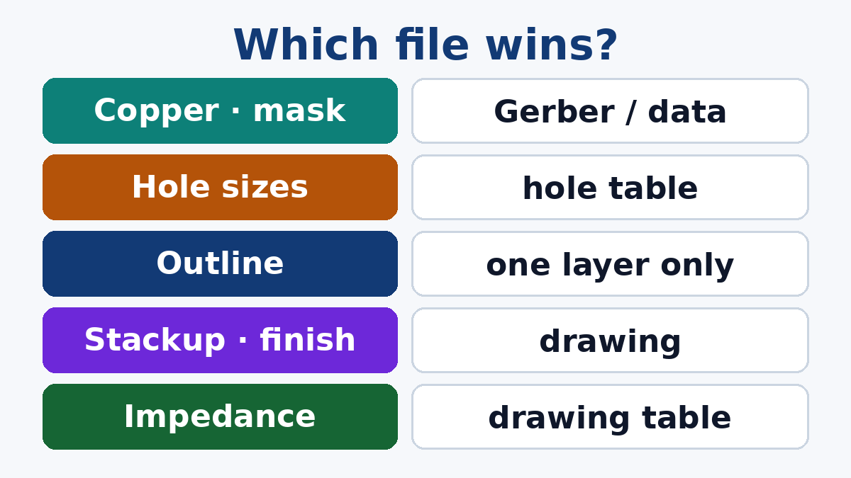
Which file wins? Decide it before CAM has to ask
A data package is a set of overlapping descriptions of the same board. The outline appears in a Gerber layer and on the drawing. Hole sizes appear in the drill file and in the drawing's hole table. Thickness appears in the stackup, on the drawing and sometimes in the job file. Where descriptions overlap, they will eventually disagree, and the factory needs to know which one rules.
A short precedence statement on the fab drawing settles it. A common, sensible arrangement:
- Copper, solder mask and legend geometry: the Gerber or intelligent data rules.
- Hole sizes: the drill file defines locations; the drawing's hole table defines finished sizes, plating and tolerances. State clearly whether sizes in the drill file are finished or drilled sizes, because the factory adds an allowance for plating.
- Board outline and mechanical features: define one authoritative outline. Mixing a keep-out layer, a mechanical layer and a dimension drawing, all slightly different, is a classic source of queries.
- Stackup, materials, thickness and finish: the drawing or stackup document rules, by named material or IPC-4101 specification sheet.
- Impedance: an impedance table on the drawing, listing layer, structure, target and tolerance, with permission for the fab to adjust trace widths within a stated range. If impedance matters, our impedance control PCB page explains what the factory will model and measure.
Without a precedence statement, a CAM engineer who finds a conflict must stop and ask, because guessing wrong produces scrap.
The cross-checks a factory runs
When a package arrives, CAM does not only check each file in isolation. These comparisons are where most problems surface.
Layer count and order versus stackup. The number of copper layers in the data must match the stackup, and the stackup order must match the file functions. With plain Gerbers this relies on names and a layer map; a missing inner layer or two layers swapped in naming is not always obvious from the images alone.
Drill file versus copper. Every plated hole should land on a pad in each copper layer it connects to, and annular ring is checked against your stated class. Plated and non-plated holes in a single file, without a clear way to tell them apart, will produce a query. So will slots defined only as a line on a mechanical layer.
Thickness arithmetic. Cores, prepregs, copper and the finish should add up to the requested finished thickness within tolerance. When they do not, the factory proposes its own construction; if you need a specific one for impedance or rigidity, say so.
Netlist versus Gerber. If you provide an IPC-D-356 netlist, or the netlist is embedded in ODB++ or IPC-2581, the factory compares your design connectivity with the connectivity extracted from the copper images. A mismatch can reveal a real defect in the export, such as a missing plane connection or a polygon that did not repour, before a single panel is made. The same netlist then drives electrical test, whether by fixture or by flying probe testing. A netlist from an earlier revision is worse than none, because every difference becomes a query.
Solder mask and paste versus copper. Mask openings should match pads with the expected clearance; paste openings should match SMD pads, with any deliberate reductions or window patterns intended rather than accidental.
For assembly, a second set of comparisons runs:
- BOM versus centroid file: every designator placed in the centroid file should appear in the BOM, and the reverse, except for lines marked do-not-populate. Count mismatches are among the most frequent assembly queries.
- Centroid versus Gerber: coordinates must share the same origin and units as the copper data, and rotations must follow a stated convention. A centroid file exported from a different origin places every part in the wrong position, consistently.
- BOM versus footprints: the package of the specified part should fit the footprint in the data. A 0603 part on an 0402 footprint is caught here, if it is caught at all before the line.
- Polarity: assembly drawing marks, silkscreen marks and footprint pin 1 should agree.
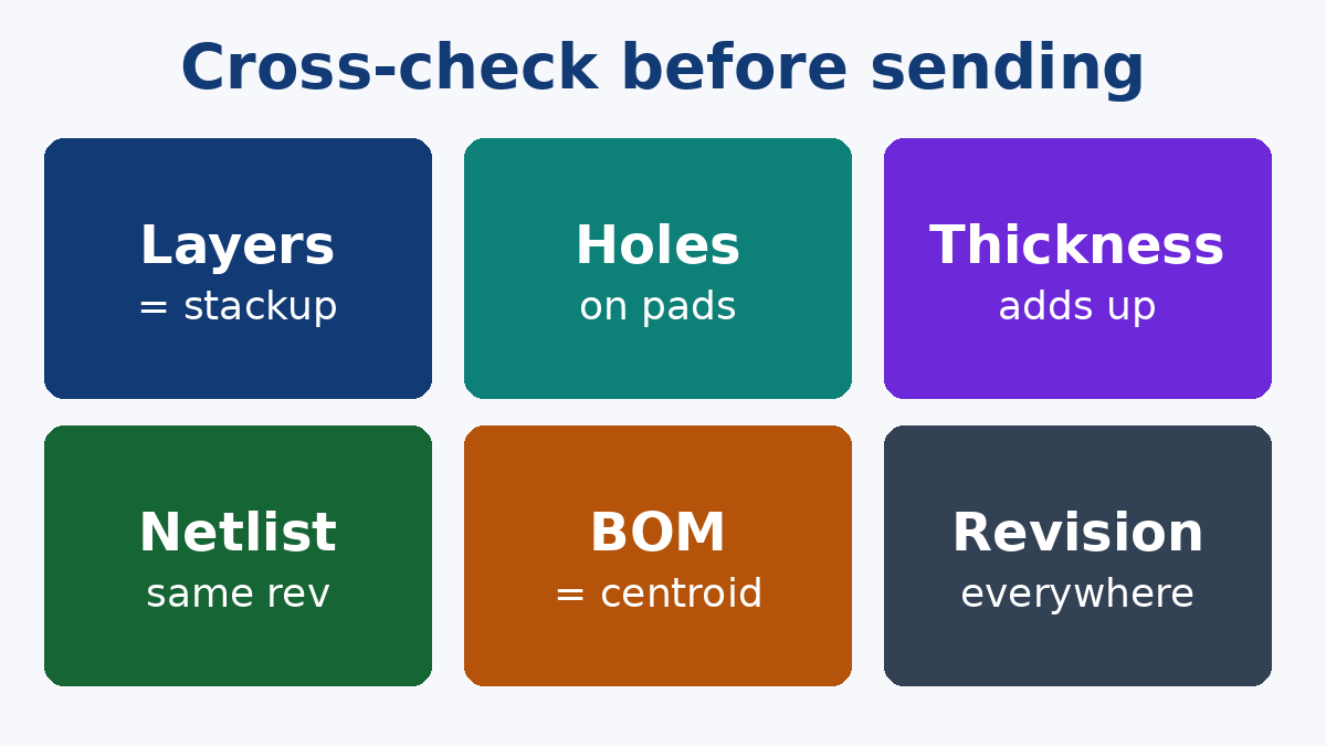
Revision control is part of the file requirement
A surprising number of conflicts are not design errors at all, but files from different revisions zipped together. A few habits prevent most of them:
- Export everything from one design revision, in one session, and package it as one archive whose name carries the part number and revision.
- Put the revision in the copper or legend as text where space permits, so a physical board can be traced back to its data.
- Put the revision on the drawing and in the BOM header, and keep them identical.
- When you resend after a change, resend the complete package, not one corrected file, and say what changed.
- Keep a short readme listing files, their function, the format, units, origin, and the precedence statement if it is not on the drawing.
What the drawing still has to say
Even a perfect intelligent data set rarely carries everything a factory must know. The fab drawing or notes should state at least:
- Material by name or IPC-4101 sheet, minimum Tg if it matters, and any halogen-free or other requirement.
- Finished thickness and tolerance; copper weights per layer.
- Surface finish and, where relevant, thickness requirements.
- Solder mask and legend colors and type.
- IPC-6012 performance class and IPC-A-600 acceptance class.
- Impedance table, if any.
- Hole table with finished sizes, plating, tolerances; any via filling or plugging requirements.
- Outline tolerances, panelization requirements if you specify them, and any special markings such as date code or UL mark.
- Test requirement, typically 100 percent electrical test against netlist.
For PCBA add an assembly drawing with polarity and orientation for anything not obvious, special process notes (conformal coating areas, glue, press-fit, torque), the workmanship class to IPC-A-610, and test requirements.
A ten-minute self-check before you hit send
Open the package in a viewer that is not your design tool, the way the factory will:
- Do all layers load, aligned, with the expected count and order?
- Does every plated hole sit on pads, and are non-plated holes identified?
- Is there exactly one board outline, closed?
- Does the stackup add up to the drawing's thickness?
- Do the drawing, BOM, archive name and copper text carry the same revision?
- Do BOM designators and centroid designators match, apart from documented do-not-populate lines?
- Do a few centroid coordinates land on the right pads when overlaid?
- Is the netlist from this revision?
- Is there a precedence statement?
- Is every requirement that cannot be drawn written down?
Our Manufacturing Files page lists what to include for PCB and PCBA quotes. This self-check is what makes that list work: when the files agree with each other, a factory can move straight from receipt to fabrication instead of a round of questions. If you would like a second set of eyes before release, send the package to us and our CAM team will return any conflicts it finds as a single list.