
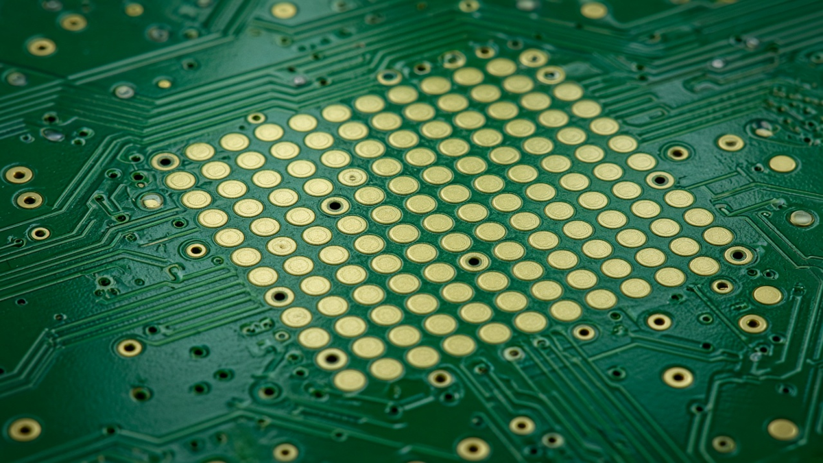
Via fill encyclopedias compare resin, conductive paste, and electroplated copper as if the buyer’s job were picking a favorite material. Overseas programs actually lose money when fill is ordered where tenting would have done—or when via-in-pad ships without a filled-and-capped class, and solder disappears into barrels at first reflow. The useful freeze is not a materials brochure. It is when fill is forced by assembly and density, which finished structure the RFQ names, which process sequence traps to ban, and what FA must accept for dimple, void, and planarity.
This article is that freeze. Hole-class naming (PTH, NPTH, via, slot) lives in PCB hole types on the RFQ. Barrel integrity before fill depends on the PTH electroless copper reliability gate. BGA escape patterns that create via-in-pad pressure live in BGA escape routing. Microvia stack logic lives in HDI PCB stackup DFM. Here the question is narrower: forced vs optional fill, RFQ class callouts, process traps, failure modes, and an acceptance matrix.
Fill is a finished structure—not a checkbox next to “via”
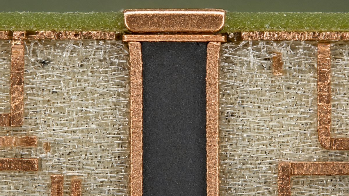
A plated via is a copper barrel. Fill occupies (some or all of) the interior. Cap plating may then put copper over a planarized fill so a pad can sit on top. Tenting only covers the opening with mask while the hole stays hollow. Plugging may close an opening without a full-depth fill. Buyers who write “filled vias” without saying filled / plugged / tented / filled-and-capped invite the cheapest interpretation that still looks green on a capability slide.
IPC-4761-style type language (filled; filled and covered; filled and capped) describes the finished protection structure. It does not by itself name the fill material. Always specify structure and material separately when both matter—or specify the assembly outcome (via-in-pad solderable flat pad) and let the plant propose a structure that meets it, in writing.
When fill is forced vs optional
Forced (or strongly forced) by assembly
Treat fill-and-cap (VIPPO / plated-over filled via class) as forced when:
- The via sits inside an SMD pad that must hold solder volume (BGA, LGA, fine QFN thermal strategies that print over vias).
- Vacuum or aggressive reflow would otherwise drain paste into open barrels and starve joints.
- Fine-pitch VIP is the only escape that meets density after fanout review.
In these cases, solder-mask plugging alone is not a substitute. Mask plug does not give a reliable flat copper pad.
Often optional (do not auto-upgrade)
Fill may be optional when:
- Vias sit outside pads and mask tenting or plugging meets contamination/solder-wick goals.
- Thermal via arrays under a pad are intentionally open (or only partially filled) per thermal design—and paste volume is managed another way.
- Buried vias need fill mainly for later lamination flatness—structure may be fill without outer copper cap (different class than VIPPO).
Forced by HDI stack—not by marketing
Stacked microvias often require electroplated copper fill (or an approved equivalent process) so the next via can land on a solid or capped intermediate. That is a build-up force, not a material fashion choice. Name the via stack on the RFQ; do not write “copper fill preferred” without the stack sketch.
Cost discipline
Fill only the vias that need the structure. Blanket “all vias filled and capped” on a dense board is a cost and yield multiplier. Call out which drill tools / which nets / which pad groups require fill-and-cap vs tent vs open.
RFQ fill-class callouts that change the quote
| Callout | What to freeze | Trap if missing |
|---|---|---|
| Structure class | Tented / plugged / filled / filled+covered / filled+capped | Plant picks cheapest hollow tent |
| Material class | Non-conductive resin / conductive paste / electroplated Cu — if you care | Resin quoted when you assumed Cu fill |
| Location | VIP under packages vs thermal array vs buried only | Whole board filled |
| Planarization + cap | Required Y/N for solderable pads | Fill without usable pad |
| Dimple / bump limit | FA acceptance (method + limit class) | Arguments after stencil design |
| Void policy | Microsection sample plan if reliability-critical | Invisible incomplete fill |
| Via list | Tool numbers / net notes / DXF of VIP set | Over-processing |
| Sequence ownership | Fill after reliable plate; no silent skip of desmear/plate | Fill over weak barrel |
Ask every bidder to restate structure class for the VIP set in one line. Quotes that only say “via fill available” are not VIPPO quotes.
Process sequence traps (buyer-visible)
Fill quality rides on earlier steps. Buyers do not run the line, but they can ban silent shortcuts in the RFQ:
- Barrel first. Electroless + electrolytic wall integrity before fill. Filling a poorly plated barrel hides the problem until thermal cycle cracks it—see the PTH electroless gate companion.
- Clean and dry. Contamination and moisture drive voids and adhesion loss under caps.
- Fill → cure → planarize → secondary metallization → cap for capped structures. Skipping planarization leaves dimples that steal solder.
- Do not confuse paste copper with electroplated copper fill. Particle+binder networks are not continuous plated copper; HDI stacked microvia assumptions often need the plated route.
- Mask plug is not planar copper. Using mask plug under BGA pads to “save fill cost” is a classic first-reflow failure.
EQ red flag: plant proposes “mask plugged VIP” for fine-pitch BGA without a written risk acceptance from the customer.
Failure modes the acceptance matrix must name
Dimple → solder starvation
A depression over the filled via reduces local paste volume after print. Fine-pitch BGA balls over dimpled VIP show opens or weak joints that look like “paste problem” or “stencil problem” but started as fill planarity.
Incomplete fill / voids
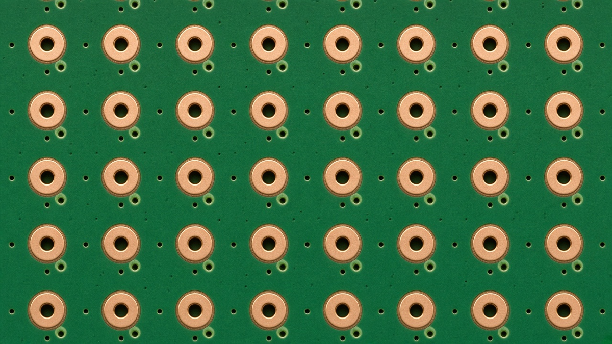
Trapped air, wrong viscosity, or out-of-window aspect ratio leave cavities. May pass electrical test (barrel still connects) and fail later under reflow or thermal cycle. Distinguish fill voids from plating voids in the copper wall—different process owners.
Outgassing / blow holes
Moisture or volatiles in fill or laminate vent through pads in reflow, disturbing solder. Bake and material control matter; RFQ should allow plant bake notes when VIP density is high.
Cap adhesion failure
Weak planarization or dirty interface → cap lifts or cracks. FA tape or microsection on sample VIP pads catches this earlier than field returns.
Resin recession
Fill drops below surface after cure or cycle → late dimple. Material CTE and cure control; acceptance should allow check after thermal stress if the product demands it.
Wrong class under thermal pads
Open thermal vias that were supposed to stay open get filled (hurting or helping depending on design)—or VIP thermal pads expected flat remain open and steal solder. Freeze intent per pad group.
Tent / plug / resin+cap / Cu fill: decision table (outcome-based)
| Assembly / build outcome needed | Typical structure direction | Usually not enough |
|---|---|---|
| Keep junk/solder out of non-pad vias | Tent or mask plug | Full Type-VII cap |
| Flat solderable pad over via (VIP) | Resin fill + planarize + Cu cap (VIPPO class) | Tent / shallow plug |
| Stacked HDI microvia landing | Electroplated Cu fill per stack plan | Mask plug |
| Thermal array, paste managed elsewhere | Open plated vias or selective fill per thermal note | Blanket cap of entire array |
| Buried via flat for later lamination | Fill (cap may be unnecessary) | Outer VIP class on buried holes |
Do not pick conductive paste because it “sounds more electrical.” For VIP planarity, non-conductive resin + copper wall + copper cap is the common workhorse; paste and plated Cu fill serve other windows. Confirm with the plant’s process book for your hole size and aspect.
Aspect ratio and hole size: silent process windows
Fill processes have diameter and depth windows. Deep high-aspect through-vias are harder to fill completely than shallow laser microvias (which use different chemistry). If your VIP sits on thick boards with small drills, require the plant to confirm fill capability for that tool size—or redesign to microvia VIP / larger pad vias. Cost traps around via and finish often hide here; see site cost-trap content when quoting dense VIP on thick stacks.
RFQ acceptance matrix (paste and fill)
| Row | Proto | Ramp | Volume |
|---|---|---|---|
| VIP structure class named | Required | Frozen | Frozen + ECO |
| Via list / tools for fill-cap | Sketch OK | Exact | Exact |
| Dimple/bump method | Agree | Measure sample | SPC or sample plan as agreed |
| Microsection of filled VIP | Sample | Sample + worst tool | Per quality plan |
| Electrical opens on VIP nets | All | All | All |
| False “mask plug OK” ban | Written | Written | Written |
| Cap adhesion check | Sample | Sample | As plan |
| Solder FA on first BGA | Engineering | Production-intent | Locked |
Attach the matrix to the RFQ. Require the quote to price VIP fill-cap set separately from commodity tenting so you see the real adder.
Quote traps
| Trap | What happens | Buyer counter |
|---|---|---|
| “Via fill” without structure | Tent delivered | Name filled+capped for VIP |
| Mask plug sold as VIPPO | Solder drain at reflow | Ban in writing |
| All vias filled | Cost blowout | Subset by tool/net |
| Cu paste assumed = plated Cu fill | HDI stack risk | Name process for microvias |
| No dimple limit | Stencil fights FA | Freeze measure |
| Fill without plate integrity | Latent barrel crack | Barrel process + section |
| Class change after stencil | Paste volume wrong | ECO before tool change |
Interaction with BGA escape and HDI
Via-in-pad is often the residue of an escape strategy. Before freezing fill on hundreds of pads, ask whether escape can move vias off pad (BGA escape routing) and save fill cost—or whether density forces VIP and therefore forces fill-and-cap. For microvia stacks, freeze fill as part of the HDI structure, not as an orphan note.
Stencil and FA: close the loop after fill is frozen
A filled-and-capped VIP pad is only as good as the paste that lands on it. After the fab freezes dimple limits, the assembly side must:
- Design stencil apertures assuming the accepted pad topography, not a perfectly flat CAD pad.
- On first article, correlate open BGA balls to VIP locations—dimple maps and SPI height maps should be compared before blaming placement.
- Ban unilateral fab changes to fill material or planarization recipe after the stencil is cut; that is an ECO that may need aperture review.
Buyers who own both fab and CM contracts should put the same VIP via list and dimple acceptance on both travelers. Split ownership without shared notes is how fab “passes fill” and CM “fails solder” with no common language.
Selective fill maps beat blanket notes
Gerber notes that say “fill all vias” are easy to write and expensive to run. Prefer a selective map:
- VIP under named packages (reference designators).
- Thermal pad vias with explicit open vs filled intent.
- Buried/blind tools that need fill for stack reasons only.
Deliver the map as a drill-tool list plus a short fab drawing note. CAM can price and panelize to that set. When engineering adds a new BGA late, update the map under ECO—do not assume the plant will infer new VIP from copper alone.
What to decide before the next VIP-heavy PO
- Which vias are inside solderable pads—and is VIP forced or avoidable by escape?
- What finished structure do those pads need (almost always fill + planarize + copper cap for fine pitch)?
- What material/process class does the plant propose for that structure—and does it match HDI microvia needs if any?
- Which vias stay tented/open—explicitly, to stop blanket fill?
- What dimple/void/cap acceptance will FA run, with method?
- Does the quote line-item the VIP set separately and restate the structure class?
Fill material catalogs do not prevent solder starvation. A forced-vs-optional decision, a named structure class, banned mask-plug-as-VIP shortcuts, and an acceptance matrix do. When pitch, board thickness, or via tools change, reopen the freeze; do not inherit last product’s “all vias resin filled” habit onto a board that only needed a small VIP set—or the reverse.