
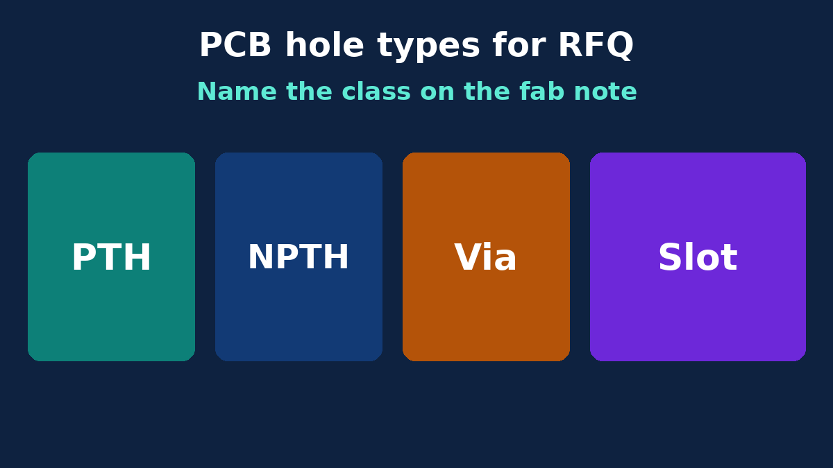
Hole charts fail RFQs when the drawing names diameters but not hole classes. A China fab quotes and programs from plated vs non-plated, through vs depth-limited, round vs slot, and whether a plated barrel will later be back-drilled. Bit catalogs and laser recipes belong elsewhere; this post is the taxonomy buyers must freeze on fab notes before the drill file is trusted.
Two axes that decide process—and cost
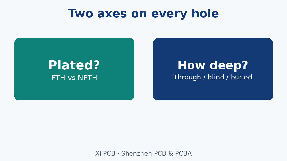
Every production hole sits on two axes at once:
- Electrical role: plated (PTH family) vs non-plated (NPTH).
- Geometry / depth: full through, blind, buried, controlled-depth (including back-drill), or non-round (slot, countersink, counterbore).
Mixing the axes on one callout—“via Ø0.3 mm”—without plating intent or finished vs drill size is how CAM opens an EQ. Name both axes.
PTH family: finished size is not the drill size
A plated through hole carries copper on the wall so layers connect. Finished hole diameter after plating is smaller than the drilled diameter. On the RFQ / fab note, lock:
- Finished hole (and tolerance class) or clearly labeled drill size plus plating allowance context.
- Whether the hole is a component hole (pin + solder) or a via (interconnect only). Same plating family; different pad, annular-ring, and assembly expectations.
- Miniaturized interconnects that are laser microvias or mechanically drilled small vias—say which. Do not bury “microvia” as a marketing adjective without stack and capture-pad rules.
NPTH must be called out as non-plated (and usually tented or plugged per your mask rules). Mounting, tooling, and foolproof holes that arrive as PTH by accident waste plating and invite shorts to chassis hardware.
Blind, buried, and through—depth is a process gate
Through holes span the finished board. Blind start on one outer surface and stop inside. Buried live only between inner layers. Each choice changes lamination sequence, registration risk, and whether mechanical or laser drill is even available on that stack. For RFQ:
- List blind/buried by start–stop layer pair, not only diameter.
- Separate mechanical blind from laser microvia when both exist on the same board.
- Do not treat a cavity or pocket floor as a “back-drill substitute”—depth-controlled features that are not stub removal need their own callout (see our cavity / back-drill notes elsewhere).
Slots, countersink, and counterbore as hole classes
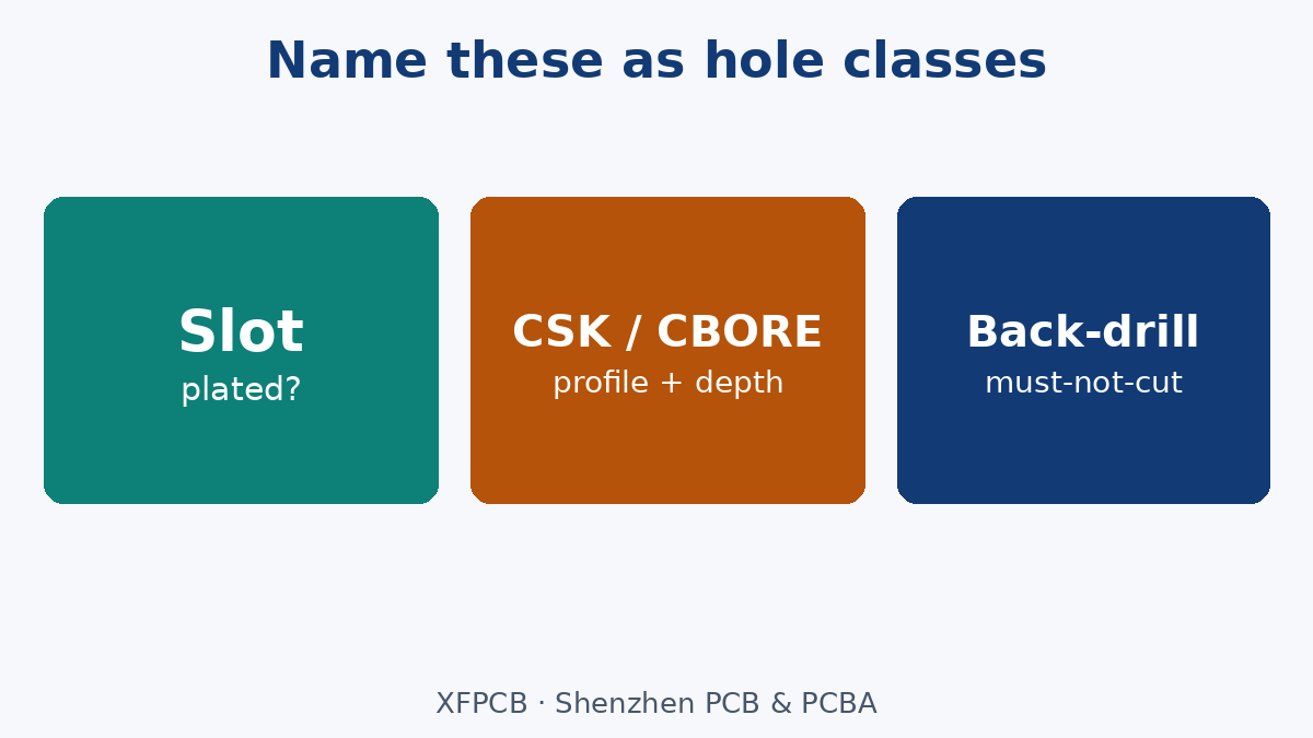
Slots are non-round openings—often overlapping drills or routed windows. State plated vs non-plated, finished width × length, corner treatment, and whether the slot seats a connector body or a fastener. Ambiguous “oval hole” language forces CAM guesses.
Countersink and counterbore are depth-and-profile classes for screw heads. They are not vias. Put angle / diameter / depth (or a referenced shop standard) on the fab note, and say whether the feature is plated. Leaving them as a 3D model only is a common overseas RFQ miss.
Back-drill as a hole class, not a comment
Back-drill removes unused plated stub after the through via is formed. Treat it as its own class on the drill chart: target via, larger back-drill diameter, depth or “must-not-cut” layer, and residual stub allowance if you own one. Signal-integrity depth math and stub failure modes are covered in dedicated posts; here the buyer job is to name the class so it is not programmed as a second full through drill.
Plant-internal holes vs drawing holes
Factories also drill registration, tooling, rivet, and coupon holes on the panel. Those belong to the process traveler, not your part drawing—unless you supply a panel drawing. Do not copy encyclopedia lists of code holes and tail holes onto a product fab note; focus on holes that define the bare board you buy.
What to put on the fab note (buyer checklist)
- PTH vs NPTH for every hole tool (and vias vs component holes).
- Finished hole vs drill language—one convention, consistently.
- Blind/buried start–stop layers; microvia vs mechanical where relevant.
- Slots and CSK/CBORE as named classes with plating intent.
- Back-drill tools with must-not-cut / residual stub fields when used.
- Tolerance only where function needs it (press-fit, precision NPTH)—not on every via.
Our PCB Fabrication Process page maps drill into the broader flow; HDI PCB covers microvia stacks when density forces laser. For stack and layer-count context on complex builds, see the Multilayer PCB Guide.
What this article is not
Not a drill-bit ST/UC or geometry catalog, not a laser-parameter guide, and not a back-drill SI deep dive. No invented hit counts, capability rankings, or hole-count price tables. Freeze the names and classes on the note so the quote and the CNC program describe the same board.