
Ground-plane advice that stops at “pour copper and avoid splits” leaves the EMI and RF failure modes unexplained. High-speed and RF return current does not follow the shortest wire—it follows the path of least impedance under the trace. When that path is broken by a slot, a connector cutout, or a missing stitch via after a layer change, loop area grows, common-mode current rises, and the board that passed DRC fails radiated or conducted tests. This article owns return-path and EMI-RF behavior tied to layout plus fab notes. It is not the fab-continuity / copper-balance post; that sister note covers press-out and etch balance. Here the question is: will the return current stay under the signal, and what must the drawing freeze so the plant does not reinterpret your reference plane?
Buyer decision frame: what “good ground” must mean on the PO
Overseas hardware and procurement teams usually inherit a stackup with one or more GND layers and a pile of copper pours. Before you RFQ, decide which of these you are actually buying:
- Dedicated reference plane(s) for impedance-controlled nets and RF sections.
- Intentional domain joins (if AGND/DGND or chassis/signal are split)—not accidental moats.
- Stitch and fence rules only where connectors, shields, or RF edges need them.
- Keep-solid zones under USB, HDMI, Ethernet, antenna feeds, and clock escapes.
If none of that is written, CAM will treat every pour as free copper. The plant can still build a beautiful panel—and ship a board whose return path is a detour around every anti-pad field. Put return-path intent on the fab note and stack table the same way you freeze finished copper weight and impedance coupons. For layer-count context when you need a true internal plane rather than a fragmented two-layer pour, see 4-Layer PCB and Multilayer PCB Guide.
Physics that matters: return current, loop area, and least impedance
At DC and low frequency, return current spreads across the plane looking for low resistance. As edge rates rise, inductance dominates: the return crowds under the forward trace because that geometry minimizes the magnetic loop. Loop area is the geometric product of how far the forward and return paths separate. Larger loop area means more radiated magnetic field and more susceptibility to incoming fields. That is why a continuous plane under a microstrip or stripline is not aesthetic—it is the return conductor.
Three layout moves inflate loop area in production boards:
- Routing across a plane split or slot so the return must go around the gap.
- Changing layers without a nearby ground via, so the return cannot hop with the signal.
- Cutting the plane under a connector or module so common-mode current on the cable shield has nowhere coherent to dump.
None of these show up as a DRC error if the clearance rules are met. They show up as EMI chamber time and late EQ. Treat continuous reference under critical nets as a design requirement, not a nice-to-have pour.
Slotted returns: when “isolation” becomes an antenna
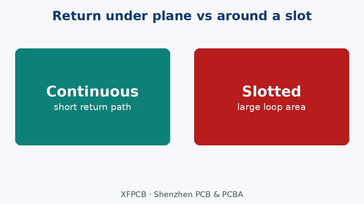
Slotting a ground plane to “keep digital noise out of analog” is one of the most common EMI own-goals. A slot forces return current to travel the long way around. The loop that forms between the signal and that detour radiates; the slot edges can also support unwanted resonances. Isolation that actually helps is usually physical zoning—place noisy and quiet circuits in different board regions—while keeping a continuous reference underneath each zone’s signals. If you must split domains:
- Document the single controlled join (net-tie, bridge component, or defined metal).
- Keep each signal class over its own reference; never cross the gap with clocks, differential pairs, or RF.
- Call the split a feature on the fab note so CAM does not “heal” it with copper thieving or fill.
Connector and BGA anti-pad fields already swiss-cheese the plane. Adding decorative isolation moats on top of that is how return paths disappear. Prefer keep-solid language under interfaces: “no plane cutouts under connector footprint except required anti-pads.”
Layer change and stitching: the return must hop too
When a signal via takes a net from L1 to L3, the return that was on L2 must find a path to the new reference. A ground via next to the signal via keeps that hop short. Without it, the return wanders through distant vias or plane edges—again growing loop area. Practical fab-aware rules:
- Place at least one GND via near each high-speed signal via at a layer change.
- For RF microstrip edges and shield cans, use via fences (stitched walls) so energy does not leak into adjacent cavities.
- Do not invent a universal millimeter pitch table for every board; pitch intent belongs to the EMC/RF owner and should be named on the drawing where it is functional.
- Remember stitch density steals routing channels and adds drill count—cost and registration risk on dense multilayer work. Stitch where physics needs it; do not spray vias “for luck.”
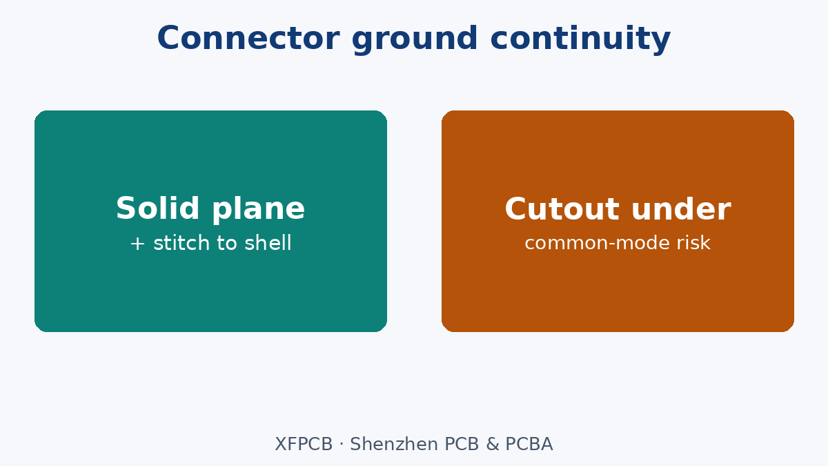
Near connectors the stitch question is sharper. Cable shields and connector shells inject common-mode current. A solid plane under the connector, tied with short vias to the shell ground pins, gives that current a defined dump. A cutout “for clearance art” under the connector is a common-mode amplifier. Put connector ground continuity on the layout checklist and on the fab keep-out note.
RF sections: microstrip, stripline, and reference discipline
RF and microwave sections make the ground plane part of the transmission line. Microstrip needs a continuous reference beneath; stripline needs continuous references above and below. Impedance is set by trace geometry and dielectric height to that plane—see Impedance Control PCB when coupons and stack notes must lock that geometry. Gaps under RF traces shift impedance and radiate. Via fences along RF corridors reduce cavity coupling; floating copper islands near RF become parasitic radiators—remove them or stitch them solidly to the main ground.
Material choice (low-loss laminates, controlled Dk) matters for insertion loss and phase, but it does not forgive a broken return path. A premium RF laminate with a slotted ground under the feed still fails radiated tests. For construction context on RF builds, High Frequency PCB sits next to this layout discipline—not instead of it.
Failure modes buyers actually see
Map symptoms to return-path causes so EQ is specific:
- Failed radiated EMI near harmonics of clocks or SERDES — often return detours from splits, slots, or missing stitch at layer changes.
- Common-mode cable noise (USB/Ethernet fails) — plane voids under the connector or weak shell-to-plane bonding.
- RF desense / degraded sensitivity — discontinuous reference under the RF path, or fence gaps that leak digital energy into the RF cavity.
- Impedance coupon passes but link margin is poor — coupon saw a solid plane; the real net crossed a swiss-cheese region.
- Analog readings jump when digital bursts — shared return constriction or a slot between domains that the digital return must cross.
Fab cannot “plate away” a layout return-path error. What fab can do is follow your solid-plane keep-outs, not fill intentional splits, and register stitch vias as drawn. What fab cannot do is invent an EMC strategy you never wrote down.
What the fab can and cannot fix
Can fix / must follow when called out:
- Honor no-route / no-split / keep-solid zones under named interfaces.
- Build the stack with the GND layers you assigned; do not silently swap which layer is reference for impedance.
- Place stitch vias per your coordinates; do not delete “extra” vias during panelization cleanup.
- Avoid copper thieving that bridges an intentional isolation gap.
Cannot fix after Gerbers are frozen:
- A high-speed net that already crosses a split.
- Missing ground vias at dozens of layer changes.
- A connector footprint with a designed cutout under the shell.
- Wrong layer count for the reference density you need (two-layer pour ≠ internal plane).
If EQ discovers a return-path hole late, the honest options are layout ECO, controlled bridge, or accepting chamber risk—not asking the plant to “add more ground somehow.”
RFQ and drawing callouts that lock return-path intent
Put these on the fab note / stackup / readme so CAM does not reinterpret:
- GND layer assignment in the stack table (which layers are solid GND vs power vs mixed).
- Impedance reference layers for each controlled net class (which plane the coupon uses).
- Keep-solid regions under connectors, RF feeds, and clock escapes—except required anti-pads.
- Intentional splits with join method named; “do not fill” language if thieving is elsewhere on the panel.
- Stitch / fence rules only where functional (connector rings, RF edges, shield cans)—not a board-wide spray.
- No floating islands in RF zones: remove or stitch.
- Finished vs artwork clarity if plane reliefs or thermal ties change local copper density near critical returns.
Also freeze manufacturing files consistently: Gerber/ODB++ plane layers matching the stack note, netlist for continuity checks, and a short English note calling out return-path keep-outs. Ambiguous “GND pour everywhere” language invites CAM optimization that seams your reference.
Common EQ loop on return-path / EMI issues
A typical overseas program cycle:
- Prototype fails radiated or desense test.
- Lab points at “grounding”; layout adds random stitch vias and copper pours.
- Respin still marginal because the slot under the connector or the layer-change without GND via was never named.
- Second EQ finally freezes keep-solid and stitch rules on the drawing—work that should have been in the first RFQ.
Break the loop by reviewing return paths before tape-out: every critical net’s reference continuity, every layer change’s nearby GND via, every external interface’s plane under the shell. Bring that checklist into the RFQ packet. Plants in China build what the notes allow; they do not own your EMC architecture unless you hired that design service.
Mixed-signal and power: returns are not the same problem
Mixed-signal boards fail EMI and noise budgets when designers treat “ground” as one net and one pour. Digital return currents want a continuous plane under fast edges. Sensitive analog returns want a quiet path that is not shared through a constricted neck with switching regulators. Those goals can coexist on one solid GND layer if placement keeps noisy and quiet circuits in different regions and each class of signal stays over copper that is continuous under its path. Splitting the plane is optional; zoning is not.
Power integrity overlaps but is not identical. A power–ground sandwich forms a useful high-frequency capacitance for the PDN, yet a clean PDN does not automatically give every signal a short return. You can pass rail ripple checks and still radiate because a SERDES lane crossed a slot. On the RFQ, name both intents when they matter: PDN plane adjacency in the stack, and signal-return keep-solid zones in the layout notes. Do not assume one copper pour solves both.
Chassis and earth connections add another layer. If the product bonds a metal enclosure or cable shield to board ground at multiple uncontrolled points, you can create loops that pick up ambient fields. Prefer documented bond points and keep the board’s signal reference continuous under the interfaces that feed those bonds. Ask assembly to confirm shield-can solder points land on the nets you intended—cans that short AGND to DGND across a planned split undo the join strategy overnight.
What to put in the English fab readme (examples of language)
Short, testable sentences beat vague “good grounding” slogans. Examples of language that CAM and EQ can act on:
- “L2 and L5 are solid GND. Do not add plane splits or copper thieving gaps under J1–J4 connector areas except antipads required by the footprint.”
- “Intentional AGND/DGND join only at net-tie NT1. Do not flood-fill across the isolation gap elsewhere on L2.”
- “Each high-speed signal via that changes reference layers shall have at least one GND via within the via cluster as drawn; do not delete stitch vias during panelization.”
- “RF corridor on L1 between markers A and B: maintain continuous L2 reference; via fence as drawn is mandatory.”
If your CAD tool exports plane layers that disagree with the stack table, fix the export before RFQ. Plants quote and CAM from the files you send; a beautiful PDF note that contradicts Gerbers loses to Gerbers.
Stack-up choices that enable or kill return paths
Layer count is a return-path decision. On two-layer boards, one side often becomes a fragmented ground pour interrupted by traces and parts. That pour is better than nothing for slow nets and is rarely adequate for fast edges or RF. Four-layer stacks with an internal GND close to the top signal layer shrink loop area for top-side routes. Six-layer and higher builds can give every critical signal layer a nearby reference—if you assign layers that way and keep those planes solid where needed. Buying more layers and then cutting them into islands wastes the money.
When impedance control is on the PO, the coupon’s reference plane must match the net’s reference plane. A coupon over solid L2 while the real net crosses a swiss-cheese L2 region is a classic false pass. Tie impedance callouts to the same keep-solid discipline used for EMI. That link is why return-path notes belong next to impedance notes in the same fab packet—not in a separate EMC memo the plant never sees.
Cost traps without inventing numbers
Return-path mistakes cost schedule and respins, not a tidy line item. Dense via fences raise drill count and can push registration risk on high layer-count boards. Unnecessary plane splits create EQ churn when CAM asks whether to fill. Over-specified stitch pitch across the whole board burns routing channels you need for the next ECO. Under-specified keep-solid zones under connectors look cheap until cable common-mode fails certification. Prefer selective, written rules over decorative copper.
Two-layer boards with a “ground pour” are especially honest about limits: a fragmented pour is not an internal plane. If EMI/RF margin is part of the product requirement, budget the layer count that gives continuous reference—then protect that reference in the fab notes.
Closing: freeze the path home
A ground plane earns its keep only when return current has a short, low-impedance path under the signal. Loop area, slotted returns, and missing stitches near connectors are layout physics problems that show up as EMI and RF failures. Write keep-solid zones, intentional joins, and functional stitch rules into the stack and fab notes so the board that ships is the reference plane you designed—not the pour CAM optimized for copper balance alone. That is the return-path / EMI-RF discipline. Continuity and copper-balance survival through press and etch remain a separate fab conversation; both matter, and neither replaces the other.
For buyers, the actionable test is simple: can a stranger in CAM point to the layers, keep-outs, and stitch features that protect return paths without guessing? If the answer is no, fix the notes before you chase another chamber date. XFPCB builds to the frozen stack and fab language you approve—bring return-path intent into that freeze, and the EMI-RF behavior you simulated has a chance to match the board that lands on the bench.