
Industrial etching is not a hobby ferric-chloride tutorial. For buyers, etch is the step that turns artwork copper into finished trace geometry—and therefore into impedance, current density, and annular-ring leftovers. This post treats etch as an impedance / geometry risk: undercut, over-etch, compensation, and what the fab note must freeze. No DIY recipes, no invented universal mil tables.
What etching actually changes
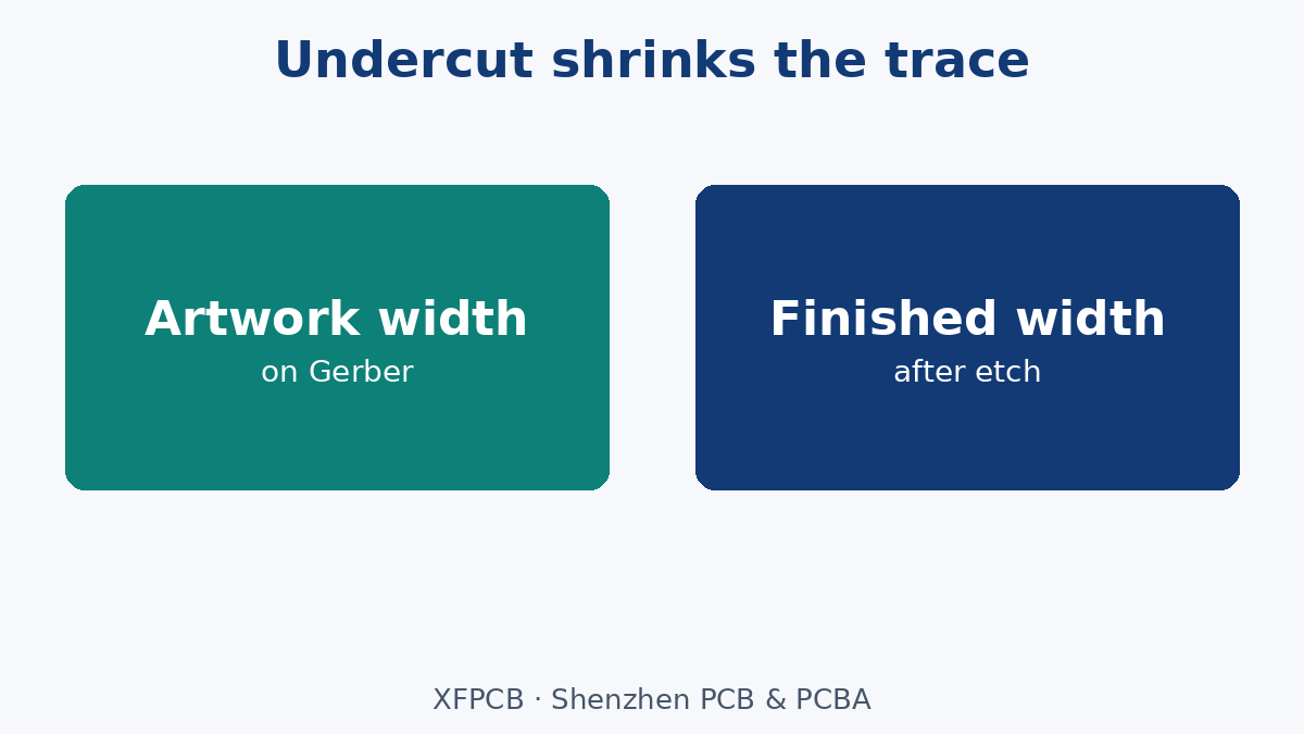
After resist defines the pattern, wet etch removes unprotected copper. Acid and alkaline chemistries, spray geometry, and copper weight all change lateral undercut under the resist edge. Finished trace width is therefore usually narrower than the artwork line unless the plant compensates (widens artwork) for the expected etch factor.
If your stackup note quotes impedance to a finished width, but the Gerber is drawn at that same number with no compensation agreement, the coupon will not match the model.
Under-etch vs over-etch—buyer-visible symptoms
Under-etch (copper left behind)
- Slivers and shorts between fine pitches.
- Impedance lower than modeled (extra copper width).
- Mask dams fighting residual copper.
Over-etch (too much copper removed)
- Traces thinner than design—higher impedance, higher resistance, open risk on hairline features.
- Pads undersized; annular ring eaten toward the drill.
- Trapezoidal cross-sections that SI models never assumed as rectangles.
Inner-layer vs outer-layer etch chemistries differ in many plants. Do not assume one compensation factor covers every layer of a multilayer.
Outer vs inner layers
Outer layers often etch with different chemistries and spray dynamics than inner layers that see alkaline systems in many shops. A fine-line outer impedance structure and a dense inner signal layer may need separate compensation stories. When the stack mixes ½ oz and 1 oz foils, say so on the note—undercut does not scale as a single slogan.
What fab notes must lock
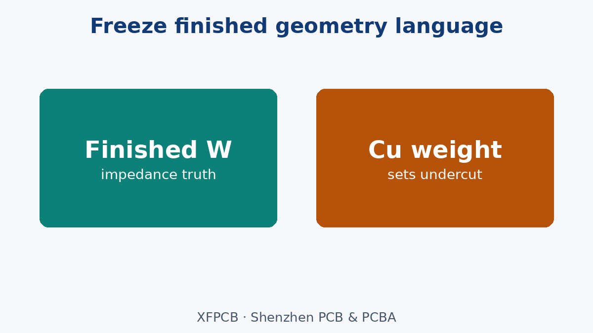
- Whether impedance / critical widths are finished dimensions (preferred) or artwork dimensions.
- Copper weight on those layers (½ oz vs 1 oz vs heavy copper changes undercut behavior).
- Minimum trace/space that the quote assumes—pushing below the quoted window is an advanced-process price, not a free CAD edit.
- Coupon locations and which stack reference they represent.
- Any customer-owned compensation table from a prior qualification—say so; do not silently re-derive.
Ask the fab how they apply etch compensation for this copper weight and resist process. You rarely need their Baumé readings; you need agreement that finished geometry is the acceptance language.
Etch and the rest of the traveler
Etch quality also inherits from imaging (LDI vs film), resist integrity, and copper foil type. Rough foils and filled resins can change edge quality. When EQ mentions “etch factor,” it is usually a geometry conversation—not a request to redesign the schematic.
Our Impedance Control PCB page is the product home for controlled dielectric and width. Process placement sits in PCB Fabrication Process. For foil and copper weight capability see Copper Thickness Capability.
What we are not claiming
No ferric-vs-cupric DIY guide, no plasma-etch parameter set, no “always compensate X mil per oz” universal rule, and no additive-print replacement pitch. Lock finished geometry language so etch chemistry stays a plant control—and your impedance coupon measures what you modeled.