
HDI is not a brochure upgrade over “more layers.” For China-fab RFQs it is a structure and DFM selection gate: you pay for laser microvias, sequential build-up (SBU) presses, registration risk, and via-in-pad fill only when BGA pitch, escape channels, board outline, and layer budget make through-hole multilayer the more expensive or impossible path. Buyers who write “HDI” without naming 1+N+1 vs 2+N+2 vs any-layer, stacked vs staggered microvias, and VIP fill/cap intent get house defaults that pass continuity and fail density, yield, or thermal life.
This page is the rigid-HDI stackup + DFM gate for engineers and procurement: when microvia density earns money; how to read build notations in buyer language; plating and reliability tradeoffs for stacked vs staggered; microvia aspect / capture pad / laser-drill chain in plain fab speech; via-in-pad (VIPPO) as an RFQ lock; why each extra SBU press raises registration and cost; practical DFM bands as confirm-with-fab guidance only; short materials notes at RFQ level; a failure map; and a checklist that blocks silent downgrade. PDN / plane capacitance / Ztarget, AS9100 vs Class language, AI-server high-layer yield, and SMT density assembly cases live on their own pages — one conceptual pointer each, not rewritten here.
When HDI earns money vs thicker through-hole multilayer
Start with geometry, not marketing.
| Driver | Through-hole multilayer often wins | HDI (microvia / SBU) starts earning money |
|---|---|---|
| BGA / CSP pitch | Coarse pitch; ample fan-out on outer layers | Pitch and pad count force blind microvias or via-in-pad to escape |
| Escape / channel | Enough layer pairs and board area for PTH dogbones | Board shrinks or I/O density chokes channels between pads |
| Board size / outline | Extra area is cheaper than another laser buildup | Outline is frozen; density must come from via architecture |
| Layer-count tradeoff | Adding 2–4 PTH layers is cheaper than one SBU cycle | Extra PTH layers still cannot escape; microvia density cuts total layers or size |
| Yield / schedule | Simple drill + plate travelers | You accept laser + fill + multi-lam risk for density that PTH cannot buy |
A practical buyer test: if a conventional multilayer with slightly larger outline or two more layers still escapes and meets impedance / thermal notes, skip HDI for prestige. If CAM already flags annular-ring starvation, dogbone collisions, or “cannot escape without blind vias,” name the build type — not “HDI capable” as a slogan.
HDI spend is laser stations, desmear/plate cycles per buildup, VIP fill/cap, extra presses, and coupon discipline. It returns value when it replaces a board that will not fit, a PTH-only layer count that will not yield, or a fan-out that forces a package change — not when the drawing only wants finer soldermask on through-hole vias.
Reading 1+N+1, 2+N+2, and any-layer (ELIC) in buyer language
Fab travelers speak in build-up counts, not encyclopedia type charts. Map them loosely so CAM and the buyer share one sentence:
| Notation (buyer language) | What it usually means on a rigid RFQ | Loose IPC-2226-style idea (not a dump of Type I–VI) |
|---|---|---|
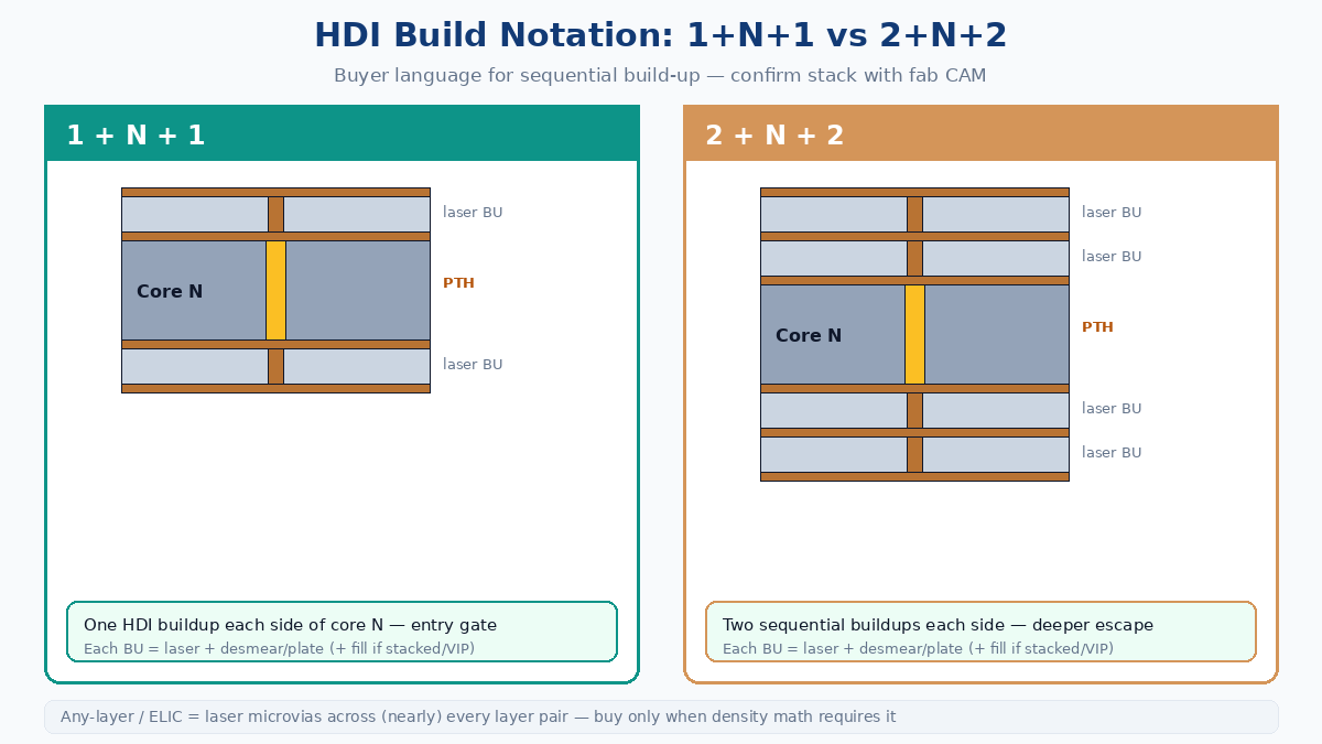
| 1+N+1 | One HDI buildup layer each side of a multilayer core N | Single-level microvia / blind structure on each face — often the entry HDI gate |
| 2+N+2 | Two sequential buildups each side of core N | Two microvia levels per side — deeper escape, more laser + press cycles |
| Any-layer / ELIC | Every (or nearly every) layer pair can take laser microvias; stacked interconnect through the stack | Highest density / registration / cost class — buy only when escape truly needs it |
N is the core (or subcomposite) layer count after the through-hole or buried structure is defined. Writing “8-layer HDI” without 1+N+1 or 2+N+2 leaves the plant free to quote a single-sided laser skin or a full ELIC stack — wildly different price and risk. Put the notation on the fab note, stackup drawing, and PO the same way.
Any-layer (ELIC in buyer decks) is not “better 2+N+2.” It is another process family: more laser hits, more fill/plate cycles, tighter full-thickness registration. Prefer 1+N+1 when one microvia level per side escapes; 2+N+2 when a second level is required. Escalate to any-layer only when density math leaves no staggered or single-level path — and expect longer EQ, more coupons, and higher scrap sensitivity.
Stacked vs staggered microvias: plating, reliability, cost
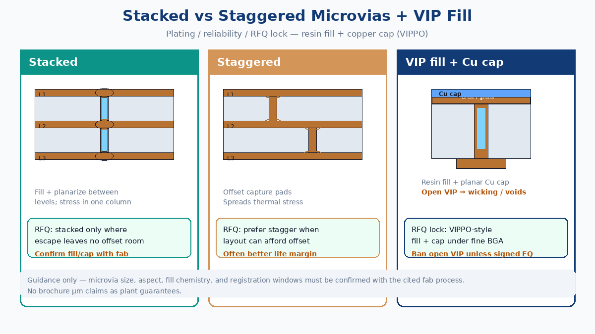
Stacked microvias sit on the same XY center through successive buildups (often with filled lower vias so the next laser lands on copper). Staggered microvias offset so each laser lands on a capture pad that is not directly over the via below.
| Theme | Stacked | Staggered |
|---|---|---|
| Density | Best vertical interconnect in smallest XY | Needs lateral offset; slightly hungrier on pad real estate |
| Process | Fill + planarize + copper-cap between levels; plating stress stacks | Each via plates more independently; fewer stacked fill interfaces |
| Reliability discussion | More interfaces (fill/cap/plate) in one column — thermal cycling and CTE mismatch concentrate here | Spreads stress; often preferred when reliability margin beats absolute density |
| Cost / yield | Extra fill, planarization, and registration to the filled land | Extra routing / pad offset; usually fewer stacked fill steps |
Prefer staggered when a few mils of offset exist and thermal cycles, multi-reflow, or Class 3-style life arguments dominate. Prefer stacked when escape leaves no offset and the fab has proven fill/cap for your copper and dielectric — confirm with that plant’s notes, not a brochure. Mixed stacks (stagger outer, stack only where forced) are fine; draw the policy so CAM does not assume every column is stacked.
Microvia geometry and the laser → desmear → plate chain
Microvias are laser-drilled (CO₂ / UV / hybrid — plant-owned) into dielectric to a capture pad, then cleaned and plated. Buyer language that helps without inventing plant recipes:
- Dielectric thickness and copper foil set the hole depth and the copper the laser must stop on or clear.
- Laser drill opens the microvia; taper and diameter depend on energy, mask, and material (laser-drillable prepreg or RCC).
- Desmear / clean removes residue so electroless or direct metallization can wet the wall and land.
- Plate builds copper on the wall (and into fill processes when VIP or stacked fill is specified).
- Capture pad / annular ring must survive registration and laser wander — undersized pads become breakout and open risks.
Aspect ratio is depth ÷ diameter. Mainstream HDI talks often stay near ≤ ~0.8:1; deeper / narrower holes starve plating and raise voids. Treat every ratio as confirm-with-fab for your dielectric and copper — not an XFPCB guarantee.
Practical discussion bands for EQ (re-confirm with the cited fab process and drawing units):
| Parameter | Mainstream HDI discussion band | Buyer lock |
|---|---|---|
| Microvia diameter | Often discussed around ~75–100 µm finished / drilled class | State diameter + finished intent; ask plant min for your dielectric |
| Aspect ratio | Often discussed ≤ ~0.8:1 | Depth from dielectric thickness ÷ diameter; flag outliers early |
| Capture pad / annular | Enough ring after registration + laser wander | Pad diameter on stackup; no “minimum pad” left blank |
| Trace / space (outer HDI) | Often discussed around ~75–100 µm / ~3–4 mil class for mainstream HDI | Call out critical nets; confirm etch capability for copper weight |
These µm/mil figures are guidance for fab confirmation only. House DFM, copper weight, glass style, and panel utilization all move the traveler — never paste them as promised XFPCB capability.
Via-in-pad: resin-fill + copper-cap (VIPPO) as an RFQ lock
Via-in-pad under BGA / CSP pads is where HDI density often lives — and where open VIP fails silently at assembly. Treat VIP fill + copper cap (VIPPO-style) as a named RFQ line, not an assumed house habit.
| Field | What to write | Fail mode if vague |
|---|---|---|
| VIP locations | Which pads / nets require via-in-pad | Shop tents or plugs inconsistently |
| Fill material | Resin / conductive fill per agreed process | Voids, wicking into pad, solder suck-out |
| Planarization + Cu cap | Copper-cap thickness intent / planar pad for SMT | Dimples under balls; open VIP after reflow |
| Open VIP policy | Forbidden under fine-pitch BGA unless signed EQ | Paste wicking, voids, head-in-pillow debates |
Open VIP (unfilled plated via under the pad) invites wicking, voids under the ball, and weak joints on small pads. Filled + capped pads give paste a planar copper surface. “VIP OK” without fill/cap language inherits whatever the last traveler used.
Sequential build-up (SBU): each press is registration + cost + yield
Every extra HDI buildup is another lamination press, another laser/plate cycle, and another chance for layer-to-layer registration to eat annular ring. Cost and scrap rise non-linearly: 2+N+2 is not “twice 1+N+1” in schedule or yield.
Buy the fewest buildup levels that escape and meet impedance / thermal notes. Skip a second buildup because a reference used ELIC when 1+N+1 still routes. Ask CAM for registration capability and coupon strategy before freezing stacked columns board-wide. “Any-layer because marketing” is an over-buy until density math is on paper.
SBU registration risk shows as breakout on capture pads, misaligned stacked vias, and impedance coupons that drift from the model — drawing and process issues, not fixed by thicker soldermask.
Materials notes at RFQ level (short)
Keep this gate short of a full substrate guide. At RFQ time name what laser and multi-lam care about: laser-drillable prepreg or RCC for buildups (standard FR-4 is not automatically laser-friendly at your diameter); high-Tg (and sometimes low-CTE) when multi-lam and lead-free reflow stack thermal stress; CTE compatibility across core and buildups for stacked-via life talks; copper foil type/weight for etch and laser stop.
Leave Dk/Df, PDN plane capacitance, and Ztarget modeling to those pages. Here materials exist so CAM can pick a laser + multi-lam capable stack that matches the build notation.
Failure map (what microsections and FA catch)
| Failure mode | Typical cause | What buyers lock to reduce it |
|---|---|---|
| Neck / knee crack at microvia | Thin plate, high aspect, thermal cycling on stacked column | Aspect band, plate/fill process, prefer stagger where possible |
| Registration breakout | SBU misregistration vs undersized capture pad | Pad size, registration capability, fewer unnecessary buildups |
| Unfilled / voided VIP | Open VIP or poor fill/cap under BGA | Named VIPPO: fill + planar Cu cap; ban open VIP on fine pitch |
| Over-stacked vias | Stacked columns where stagger would route | Stack only where density forces it; document mixed policy |
| Incomplete desmear / void in microvia | Residue after laser | Process capability for your dielectric; coupon microsection |
| Silent build downgrade | RFQ said 2+N+2; traveler shipped 1+N+1 | Identical build notation on drawing, fab note, PO; no class/build change without signed EQ |
Electrical test can beep through a starved microvia that still fails after reflow. Put coupon / microsection expectations on Class 3 or high-density HDI POs the same way PTH copper belongs on plating POs.
RFQ checklist: structure + DFM gate
Put these on the fab note and PO so CAM cannot invent a quieter stack:
| Lock | Write explicitly |
|---|---|
| Build type | 1+N+1 / 2+N+2 / any-layer (ELIC) with N defined on stackup |
| Stacked vs staggered | Policy per region or net; mixed allowed if drawn |
| Microvia size / aspect | Diameter + dielectric thickness; confirm aspect with fab |
| VIP fill / cap | Resin fill + copper-cap (VIPPO) where via-in-pad; open VIP forbidden under fine BGA unless EQ |
| Copper weights | Outer / buildup / core oz as on stackup |
| Impedance | If any — stackup + tolerance; details on impedance/PDN pages, not reinvented here |
| IPC class | IPC-6012 class + revision (product class ≠ AS9100 QMS) |
| Coupon / microsection | FA plan for microvia fill, VIP cap, registration, plate |
| No silent downgrade | No build-type, VIP, or class reduction without signed EQ |
Quote comparison is meaningless across a 1+N+1 filled-VIP board and an “HDI” label that is only one-sided laser dogbones. Normalize build notation + VIP + class before unit price.
When the drawing freezes, the gate is done: either microvia density and SBU presses buy real escape and outline, or you step back to a thicker through-hole multilayer CAM can yield. That decision — not the word “HDI” on a datasheet — is what China-fab RFQs should record.