
Industry primers that list three density levers — finer lines and spaces, more layers, and smaller vias — then dwell on copper-foil roughness and adhesion tradeoffs still leave export buyers without a practice-and-RFQ frame. This page owns that frame: how to increase PCB wiring density in factory language (finer L/S, via architecture, microvia / HDI paths, layer-count vs density tradeoffs, BGA escape), and which China fab RFQ locks (min L/S, via type, stackup class) keep quotes comparable. Soft CTA only. Sibling XFPCB lanes already own the HDI density definition primer, the advantages-and-applications gate, and the stackup / DFM selection deep dive — name those lanes in prose; do not clone them. No competitor brands. No invented XFPCB minimum line/space microns, HDI layer-count claims, or fake capability dashboards.
What “wiring density” means on a fab traveler
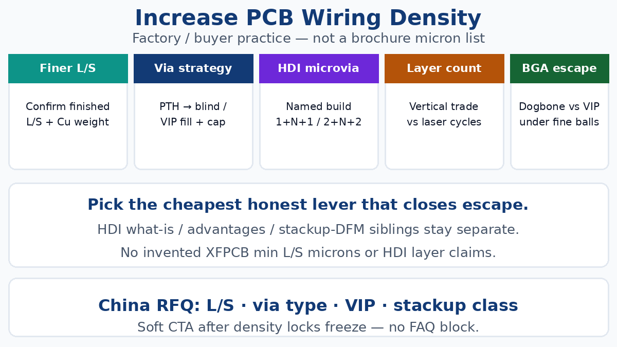
Wiring density is not a marketing adjective. In CAM and procurement speech it is how many nets, pads, and interconnect features you must place in a fixed XY outline — and whether conventional plated through-holes (PTH) can still escape them honestly. When BGA / CSP pitch tightens, outline freezes, or both faces must carry dense packages, density pressure shows up as etch feature size, via diameter and type, build-up count, and registration risk. Those are traveler fields, not brochure slogans.
Three buyer jobs often get collapsed into one soft RFQ line (“high density OK”). Keep them separate:
- Feature size — finished line width and spacing, copper weight, and etch process window.
- Via architecture — PTH vs blind / buried vs laser microvia, via-in-pad policy, stacked vs staggered.
- Stack class — conventional multilayer vs sequential build-up (for example 1+N+1 / 2+N+2 / any-layer notation), copper weights outer / buildup / core, and dielectric family notes.
A board can be “dense” on etch alone and still fail escape. Another can use microvias without needing the finest etch the plant owns. Name which job you are buying before you compare unit price.
Lever 1 — finer lines and spaces (and when not to)
The most direct horizontal density move is shrinking conductor width and spacing so more routes fit between pads and outline. Fine-line etch widens routing channels without adding layers — and it narrows the fab process window. Smooth copper foils help define fine features; adhesion, peel strength, and high-frequency conductor loss still trade with surface profile. That materials physics belongs on laminate and RFQ notes when your controlled document already cares; this page does not invent plant-specific µm menus.
Buyer practice, not brochure microns. Do not paste a marketing “25 µm capable” line onto the RFQ unless your drawing and PE already freeze that finished L/S with copper weight. Ask for the plant’s confirm-with-fab finished minimum L/S at the copper weight you will buy, plus whether LDI (laser direct imaging) is assumed on outer layers. Soft “fine line OK” language lets CAM substitute a quieter etch class after award.
When finer L/S is enough. Coarse-to-moderate BGA pitch, ample channel between pads, and an outline that still allows PTH fan-out often close with etch tightening alone — especially when you can add a little routing real estate or accept a dogbone fan-out. Spend process risk on etch before you buy sequential laser cycles.
When finer L/S is not enough. Fine-pitch balls, via-in-pad under SMT pads, or frozen smartphone-class outlines usually starve annular rings and channels before etch alone saves the design. At that point via architecture and build-up class dominate; etch is a supporting lock, not the whole density plan.
Pair critical impedance nets with an impedance-control process note when L/S and dielectric thickness both move — density without stack reference is how SI and fab quotes diverge. Do not invent XFPCB finished-micron tables here; freeze L/S + copper weight on the drawing and let bidders confirm capability against their window.
Lever 2 — via strategies that free routing channels
Vias consume pad real estate and block channels. Shrinking via and pad diameters, moving from through-hole to blind / buried structures, and placing vias in or near pads are the classic density moves after etch.
Through-hole multilayer first. Conventional PTH still wins when pitch and outline leave room for dogbone escape. Larger drills and pads are cheaper and more forgiving on registration. Prefer PTH when CAM can escape without starving annular rings.
Blind and buried vias. Blind vias connect an outer layer to an inner layer without drilling the full stack; buried vias sit entirely inside. Both free outer routing real estate and shorten some paths. They also add drill and lamination sequence complexity — name which layer pairs need them on the stackup drawing. Vague “blind OK” invites wrong depths.
Via-in-pad (VIP) / filled and capped. Placing a via in the SMT pad shortens escape and saves dogbone space under fine balls. Open vias under paste invite wicking and voids; resin or conductive fill plus a planar copper cap (VIPPO-style language on the fab note) is the usual production plan. Write fill / cap as a named RFQ line, not an assumed habit.
Stacked vs staggered. Stacked microvias share one XY center and buy the tightest footprint; staggered vias offset capture pads and often ease plating stress. Prefer stagger where a few mils exist; stack only where escape forces it. Mixed policies are normal when drawn per region.
Via diameter, aspect ratio, and fill chemistry are plant-confirmed fields. This article does not invent XFPCB drill tables. Put finished or drilled intent, dielectric thickness, and fill / cap on the traveler so every bidder prices the same hole family.
Lever 3 — HDI microvias when PTH escape collapses
When density crosses the point where conventional through-hole multilayer cannot escape pads at acceptable size or layer count, the process family shifts to HDI PCB construction: laser-drilled microvias, finer features, and usually sequential build-up (SBU). Microvias connect adjacent or near-adjacent layers to a capture pad instead of punching the full board thickness. That short path is what frees fine-pitch escape.
What this page does not own. The live “what is an HDI PCB” primer already covers density definition, microvia role, stacked vs staggered primer language, and 1+N+1 / any-layer buyer basics. The advantages-and-applications sibling owns which benefits earn money and which soft claims to refuse. The stackup / DFM sibling owns µm-level selection gates and confirm-with-fab bands. Prose pointers only — do not clone those essays here. This page only places microvias inside the broader density toolkit: use them when etch and PTH via strategies still leave escape broken.
Build notation belongs on the RFQ. Writing “8-layer HDI” without 1+N+1 / 2+N+2 / any-layer (with N defined) lets one shop quote a single laser skin and another quote a full any-layer stack. Put the build string on stackup, fab note, and PO the same way.
Cost and scrap rise non-linearly. Each extra buildup is another press, another registration chance, and another laser / fill cycle. Buy the lowest build class that closes escape — not the densest adjective on the datasheet.
Layer count vs density — the vertical tradeoff
When horizontal space runs out, adding layers is the vertical density lever. A Multilayer PCB Guide construction spreads signals across more copper planes so each layer carries fewer conflicting routes. That helps — and it makes the board thicker overall while individual dielectrics often get thinner.
What you buy with more layers. More routing planes, cleaner reference for impedance-controlled nets, and room to separate noisy and quiet domains. For many digital boards, two extra conventional layers still beat a laser buildup on cost and schedule when outline can grow slightly or pitch is moderate.
What you inherit. Tighter thickness control, more registration exposure, longer lamination cycles, and higher material cost. Thin cores on high layer counts make dimensional stability harder; even small layer-to-layer shifts eat annular ring on fine features. High layer-count programs should freeze copper weights, dielectric targets, and registration expectations — not only “add four layers.”
Trade study rule. Ask CAM whether escape closes with (a) tighter L/S on current layer count, (b) two more PTH layers, or (c) a named HDI build-up. Rank by total cost of fabrication + scrap risk + schedule, not by which option sounds most advanced. A thinner HDI skin that replaces a thick PTH multilayer can win on form factor when escape and impedance allow — treat that as a design-specific study with a drawn build string, not a universal recipe.
BGA escape — where density pressure usually shows first
Fine-pitch BGA and CSP packages are the practical density gate for most export buyers. Dogbone PTH fan-out consumes channel under and around the array; when ball pitch tightens, the fan-out collides with itself and with keep-outs before the rest of the board feels crowded.
Escape checklist (buyer-level).
- Can PTH dogbones escape at your pitch and pad size without annular-ring starvation?
- Do you need via-in-pad under balls, and is fill / copper cap named?
- Are blind microvias required on the first buildup, and is build-up type written (not “HDI capable”)?
- Is stacked vs staggered policy drawn under the array only, or incorrectly applied board-wide?
- Do outer L/S and copper weight match the escape channels CAM will actually etch?
When the answer set forces blind vias or VIP under fine balls, open the BGA PCB capability lane for process ownership and keep this article’s job as the density decision frame. Do not paste a full BGA manufacturing encyclopedia here. Freeze escape architecture before outline and layer count are treated as settled — reverse order is how late EQs reopen the stack.
China fab RFQ locks that keep density quotes honest
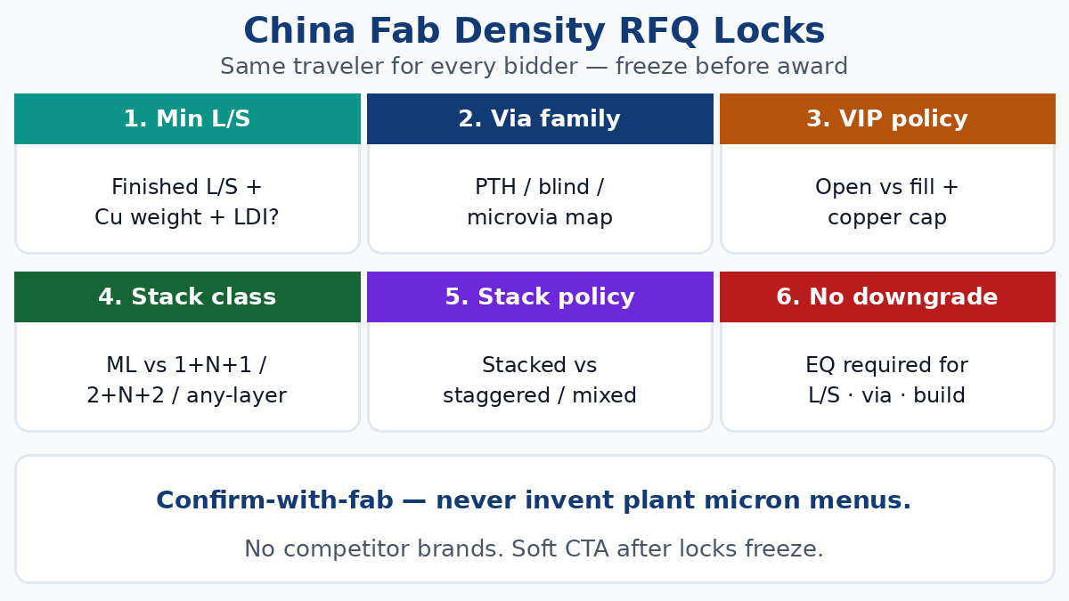
Export quotes diverge when density language stays soft (“fine line,” “HDI OK,” “BGA ready”). Paste comparable locks so every bidder answers the same traveler. Attach stackup, Gerbers, and fab notes with Manufacturing Files before “density TBD” quotes are scored as comparable.
- Finished min L/S + copper weight — confirm-with-fab finished line/space at the ounce you buy; state whether LDI is assumed. No silent etch-class downgrade without signed EQ.
- Via family — PTH / blind / buried / microvia map by layer pair; finished or drilled diameter intent; aspect tied to dielectric thickness.
- Via-in-pad policy — open vs filled; resin or conductive fill; copper cap where SMT or stacked lasers need a flat land.
- Stackup class — conventional multilayer vs 1+N+1 / 2+N+2 / any-layer with N defined; copper weights outer / buildup / core; laser-drillable buildup family when HDI skins apply.
- Stacked vs staggered policy — per region or net; mixed allowed if drawn.
- Impedance / SI nets — controlled nets, stack reference, tolerance — when density moves dielectric or L/S on those nets.
- Registration / acceptance — class (for example IPC Class 2 vs 3), coupon or microsection expectations when features are fine; no invented plant yield % as a substitute for acceptance language.
- Quantity, revision, no silent downgrade — proto vs production band; frozen Gerber / stack revision; no L/S, via-type, VIP, or build-class cut without signed EQ.
Do not invent XFPCB micron menus, HDI layer warranties, or competitor brand claims. Generic feature + via + stack locks are enough for comparable China RFQs; confirm process fit against the plant technical-capabilities menu when the construction leaves commodity through-hole multilayer.
Soft next step
Increase PCB wiring density in practice by choosing the cheapest honest lever that closes escape: tighten L/S when channels still exist, reshape via architecture before you buy lasers, add conventional layers when vertical space is cheaper than sequential build-up, and move to a named HDI microvia build only when PTH escape collapses under fine-pitch packages or a frozen outline. Put finished L/S, via map, VIP fill / cap, stackup class, and stacked policy on the China fab RFQ so every bidder prices the same traveler. Soft next step when the stack and Manufacturing Files are clear: send the package through How to Place an Order — after density locks freeze, not after a soft “high density OK” line reopens etch class and via type post-award.