
Buyer guides that stop at hot-swap vs soldered still leave export teams without a fab-ready decision frame. This page owns that frame: layer count tradeoffs, switch footprints and sockets, diode matrix hygiene, RGB / underglow power and EMI notes, FR-4 vs true flex regions, panelization and DFM, and China fab RFQ locks that keep quotes comparable. Soft CTA only. Flex-cut vs non-flex-cut feel is a separate XFPCB lane — name flex-cut here only as one design choice; do not treat this guide as that debate. No competitor brands. No invented XFPCB certificates, turnaround days, dollar menus, or capability dashboards.
What a keyboard PCB is on a fab traveler
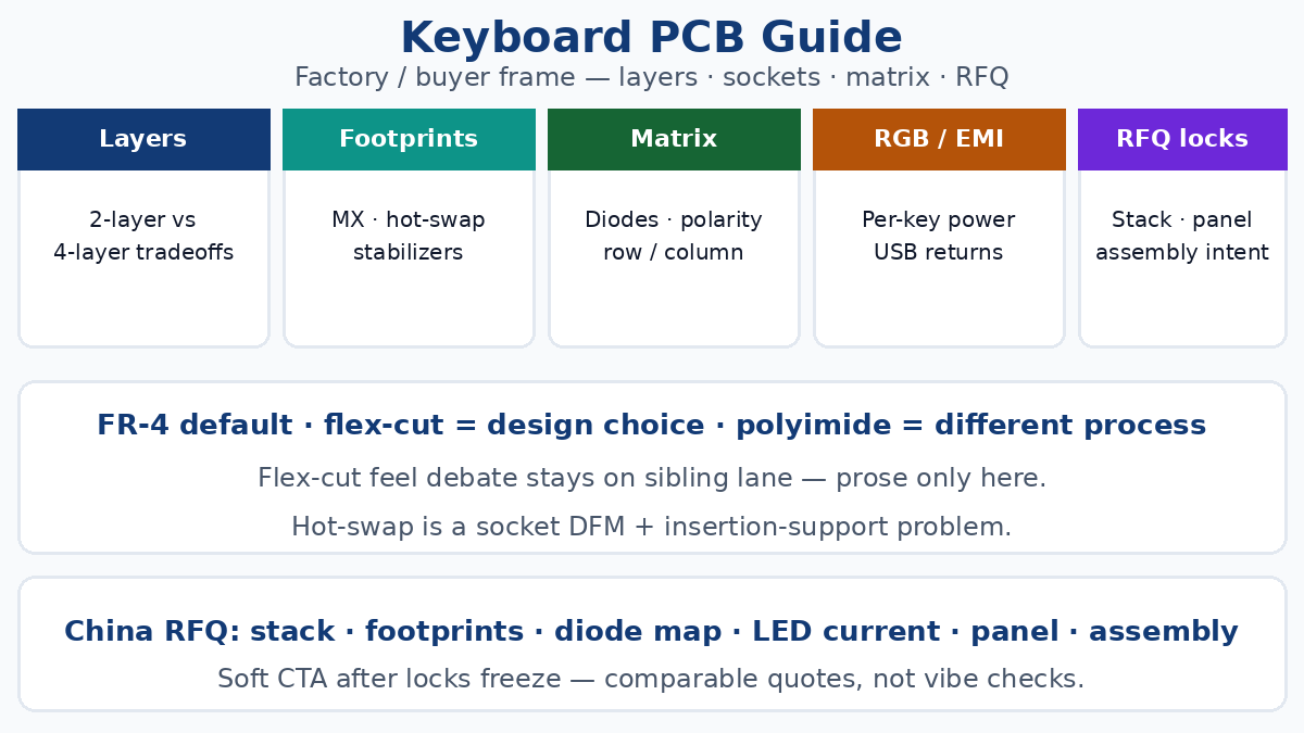
On the floor, a keyboard PCB is a rigid FR-4 (usually) interconnect that carries the switch matrix, diodes, MCU or daughter interconnect, USB or wireless front-end, and optional LED rails — not a decorative plate and not a firmware brochure. Builders care about feel and remapping. Buyers and PE care about whether the Gerber set, stackup note, footprint library, and assembly drawing can be quoted without a week of clarifying emails.
Typical traveler contents:
- Outline, mounting holes, USB cutout, and stabilizer clearances matched to case / plate drawings
- Switch footprint field (soldered pads, hot-swap sockets, or both footprints shared)
- Diode polarity and orientation map for the matrix
- Copper stack: finished thickness, copper weight, soldermask / legend, surface finish
- Optional LED footprints (per-key, underglow, or both) with current-budget notes
- Panelization preference if the fab will ship arrays for SMT
If those items are verbal or buried in a Discord thread, China fab RFQs diverge. Lock them on the fab drawing and RFQ packet.
Layer count — 2-layer vs 4-layer tradeoffs
Most mechanical keyboard PCBs ship as 2-layer or 4-layer FR-4. Layer count is not a status badge; it is routing budget, return-path quality, and cost.
When a 2-Layer PCB is enough. Sparse ortholinear or small form-factor boards, soldered MX-style footprints without dense RGB, and layouts that keep row/column routing and USB differential pair clean on two sides often stay on 2-layer successfully. Cost and lead time usually favor the simpler stack. Watch ground continuity under the USB connector and around the MCU — a broken return path on a 2-layer keyboard shows up as flaky USB and noisy LED flicker long before anyone argues about “premium layers.”
When a 4-Layer PCB earns its keep. Per-key RGB, hot-swap sockets that crowd both sides, wireless modules with antenna keepouts, dual USB or daughterboard FFC escapes, and dense full-size or Alice layouts often need inner planes for power distribution and quieter returns. Four layers also buy cleaner separation of matrix signals from LED power pours. Do not order 4-layer as marketing; order it when the schematic already has LED current, antenna keepouts, or escape density that a 2-layer copper map cannot close without gymnastics.
Thickness. 1.2 mm and 1.6 mm are common. Thickness changes stiffness and how PCB-mount stabilizers seat; it is independent of whether you later add flex-cuts. Confirm mechanical BOM before you freeze unfinished thickness on the RFQ.
Multilayer constructions beyond four layers exist for specialized interconnect, but most keyboard programs do not need them. If you are already stacking atypical layer counts for density or RF, treat that as a stack conversation under a Multilayer PCB Guide lane — not as a default keyboard SKU.
Switch footprints, hot-swap sockets, and stabilizer geometry
MX-style 3-pin vs 5-pin. Most consumer switches use Cherry MX–compatible pinouts. 5-pin plastic legs aid alignment; 3-pin switches still fit 5-pin pad maps if the two plastic-guide holes are present or unused. Footprint libraries must match the switch family you claim — pin pitch errors are painful after a thousand PCBs are etched.
Hot-swap sockets. Sockets are soldered once; switches insert and remove without soldering. That is a builder feature and an assembly / reliability constraint:
- Socket footprint, orientation, and polarity (where applicable) belong in the library and silkscreen
- Keep enough FR-4 around each socket for repeated insertion force — especially if the board later uses flex-cuts near the typing zone
- Spec socket brand / series on the BOM so SMT and rework use one geometry
- Plan support during switch install (fixture or plate) so end users do not flex pads off the board
Soldered switches. Stronger permanent joints, denser possible layouts (no socket body), and fewer mechanical wear points. Assembly must own through-hole wave / selective solder or hand solder labor. Mixed hot-swap + soldered regions on one PCB need explicit notes so the traveler does not assume one process.
Stabilizers. PCB-mount vs plate-mount changes hole maps and keepouts. Spacebar / Enter / Shift stabilizer footprints that fight switch sockets or LED holes become NPI scrap. Freeze stabilizer type with the case/plate package before Gerber release.
Diode matrix — electrical hygiene that CAM cannot invent
Keyboards scan a row/column matrix. Diodes (usually one per switch) stop ghosting when multiple keys are held. From a fab / assembly view:
- Polarity must be unambiguous on silkscreen and assembly drawing. Reversed diode fields fail whole rows or columns after SMT.
- Package choice (SOD-123, 0805 diode, through-hole axial, etc.) drives pick-and-place vs hand insert. Match package to your volume and inspection plan.
- Matrix net naming in the schematic and test plan lets flying-probe / ICT / functional fixtures map failures to a row or column instead of “board dead.”
- Unused matrix positions still need a defined state if the firmware expects a fixed layout — empty pads without diodes can be intentional; undocumented opens look like defects.
Firmware platforms (open or proprietary) are a product decision. This guide only requires that the electrical matrix on copper matches the firmware’s expected wiring — fab cannot flash away a swapped row net.
RGB, underglow, power, and EMI notes
LED features sell keyboards and punish sloppy power design.
Per-key vs underglow. Per-key LEDs multiply current and routing density under the switch field. Underglow strips along edges need continuous pours and connector or solder-pad strain relief. Mixing both without a current budget is how USB ports brown out.
Power distribution. Estimate peak LED current at the brightness you claim, not at a demo screenshot. Size planes / pours, decoupling near LED drivers or MCU LED pins, and USB inrush accordingly. On 2-layer boards, LED returns that snake through matrix territory invite flicker and EMI complaints.
EMI / ESD hygiene. Keyboards sit in user hands and plug into hosts. Keep USB differential pairs short and referenced, ESD parts near the connector if your design uses them, and LED switching edges from coupling into matrix sense lines. Wireless SKUs add antenna keepouts and ground-clear rules — put those on a mechanical / copper keepout layer the fab can see.
North vs south facing LEDs. Builder preference for shine-through keycaps is real; for fab it is only a footprint rotation and clearance check against stabilizer and switch bodies. Lock orientation in the library so a late “flip all LEDs” ECO does not appear after stencil cut.
Materials — FR-4 keyboard boards vs true flex regions
Default keyboard PCBs are rigid FR-4. That is correct for most MX-style builds.
Flex-cut as a design choice. Some boards add routed slots in FR-4 so local stiffness drops for a softer typing zone. That is still rigid laminate with intentional cuts — not polyimide flex. Feel, cut-map DFM, and hot-swap keepouts around slots already live on the flex-cut vs non-flex-cut sibling lane; here the buyer rule is simple: if you want slots, call them out as FR-4 flex-cuts with a cut map on the RFQ, and do not say “flex PCB” unless you mean something else.
True Flexible PCB regions. Polyimide flex (or rigid-flex) belongs when the product needs a dynamic or install bend — daughter interconnects, tight 3D case routing, or wearable-adjacent designs — not as a synonym for “board that feels soft.” If only a ribbon or FFC is flexible and the switch field stays FR-4, say so. Wrong-process quotes waste a week. When you truly need polyimide constructions, route that conversation through the Flexible PCB service lane with stack and bend notes attached.
Finish and mask. ENIG, HASL, and OSP all appear on keyboard programs. Hot-swap sockets and fine USB footprints often prefer flat finishes; match finish to socket and connector reliability, not to forum mythology. Soldermask color is cosmetic unless clearance or contrast for AOI matters — still name it on the RFQ.
Panelization, DFM, and assembly fixtures
Keyboard outlines are large, often irregular, and full of holes. That stresses panel design.
- Rails and tabs. Thin or heavily perforated boards need process rails so panels do not flap through etch, plating, and solder-mask. Place breakaway tabs away from hot-swap fields, USB tongues, and narrow bridges.
- Array for SMT. If PCB Assembly will place diodes, sockets, MCU, and LEDs, agree panel size, fiducials, and tooling holes before stencil. One-off single-board panels slow every SMT step.
- Warpage. Large thin FR-4 arrays warp. Set expectations for thickness, copper balance, and whether a carrier is required in reflow.
- Depaneling. Mouse bites vs V-score vs tab-route — pick a method that does not tear copper near edge LEDs or USB.
- Test coupons / e-test. Bare-board electrical test should cover matrix nets and LED rails you care about. Say whether flying-probe or fixture test is expected at the quoted quantity.
DFM is not a vibes checklist. Min hole size for switch pins / sockets, annular ring, soldermask dam between fine pads, and copper-to-outline clearance belong in fab notes with numbers your vendor accepted — not copied from an unrelated stack.
China fab RFQ locks for keyboard PCBs
Send the same packet to every bidder:
- Gerbers + drill + fabrication drawing: FR-4 (or named material), finished thickness, copper weight, layer count, soldermask / legend, surface finish.
- Explicit technology note: rigid keyboard PCB; if flex-cuts exist, “FR-4 with routed flex-cuts” + cut map — not polyimide flex unless that is the real stack.
- Switch footprint class: soldered / hot-swap socket P/N / mixed; stabilizer hole map reference.
- Diode package and polarity map; LED type and estimated peak current if RGB / underglow is fitted.
- Panelization preference: rail width, tab style, “no tabs on socket fields,” array count for SMT.
- Assembly intent: fab-only vs fab + SMT / THT; carrier required Y/N; who owns socket press-fit vs solder.
- Quantity, e-test requirement, first-article expectations (photo of sockets, USB fit to case opening).
- Revision control: which ECO absorbs layout changes before volume.
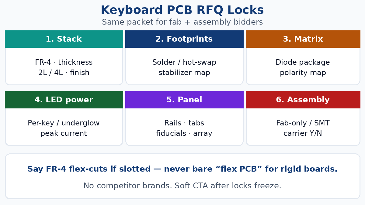
Vague RFQs that say “mechanical keyboard PCB, hotswap, RGB, quick” get incomparable quotes. Comparable quotes need the locks above. For file naming and package expectations, keep Manufacturing Files conventions consistent across fab and assembly bidders so CAM is not reverse-engineering a zip from three chat apps.
Quick-turn keyboard prototypes are normal when the stack and footprints are already frozen; rushed RFQs that still change socket series mid-quote are not quick — they are restart. How to Place an Order on the site is the commercial path once the packet is honest; the engineering path is freezing the locks first.
Soft close for buyers
A keyboard PCB succeeds when copper, footprints, matrix polarity, LED power, and panel notes match the case and firmware you actually ship — not when a brochure promises hot-swap and RGB in one sentence. Choose 2-layer or 4-layer from routing and return-path need, treat hot-swap as a socket DFM problem, keep flex-cut language precise if you use slots, and put China fab RFQ locks on paper before price shopping. When the packet is ready, route fab and assembly through a clear RFQ rather than a vibe check — that is how overseas buyers avoid wrong-process quotes and socket fields that fail the first week of switch swaps.