
Buyers ask for an “LED PCB board” when a light engine, strip, or array leaves FR-4 too hot, or when a China fab quote arrives with aluminum thickness named and dielectric left blank. This guide is the factory/buyer frame for that decision: when FR-4 is enough, when a metal-core path earns its keep, what thermal and copper notes belong on the RFQ, how white mask and reflectivity should be written without overselling, how LED arrays panelize and assemble, and which locks keep quotes comparable. Soft CTA only. A separate XFPCB lane already covers aluminum MCPCB use-cases across lighting, power, and drivers broadly — here the focus stays LED boards, FR-4 vs metal core for LEDs, and fab/assembly RFQ language. No competitor brands. No invented XFPCB capability menus.
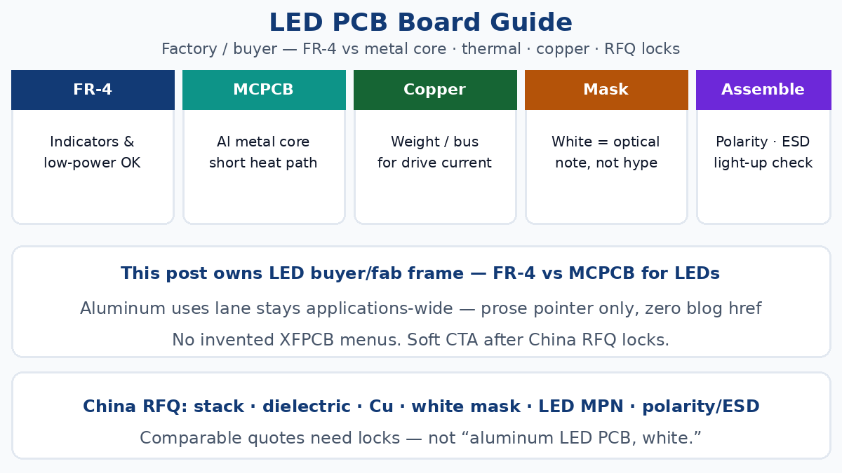
What an LED PCB board has to do
An LED PCB is still a printed circuit board: copper routes current, pads hold packages, mask and finish protect and wet. The difference is the heat and optical job. High-brightness LEDs turn a large share of input power into heat at a small footprint. Junction temperature drives lumen maintenance, color shift, and lifetime. The board is often the first heat spreader between the LED thermal pad and the housing or heatsink.
So an LED RFQ is not only “1.6 mm, white mask, ENIG.” It is a thermal path contract: how heat leaves the die, how much copper and dielectric (or metal core) carry it, how current reaches each die without voltage drop, and how the assembler places polarity-sensitive packages without ESD damage. Name those jobs early and the stack choice follows.
When FR-4 is enough for LEDs
FR-4 still wins a lot of LED work. Indicator LEDs, low-lumen status lamps, and modest backlight strings often stay inside junction limits on FR-4 with copper pours, short traces, and a sensible driver. If the watts per package are low, duty cycle is intermittent, and the enclosure already sinks heat, paying for a thermal dielectric and aluminum base is optional.
FR-4 also wins when the same board must host dense digital, multilayer routing, or double-sided connectors that classic single-sided metal-core construction fights. Hybrid products — FR-4 control board plus a metal-core LED plate — are common when the light engine needs a short thermal path and the MCU board needs layers. That split adds connectors and assembly steps; it is honest when one stack cannot do both jobs well.
Buyer language that keeps FR-4 honest for LEDs:
- Package power, ambient, and allowed junction or case temperature
- Copper weight and pour plan under LED pads (often 1 oz or 2 oz; heavier when current or spreading demands it)
- Thermal via arrays under or around LED thermal pads when heat must reach a bottom pour or chassis contact
- Heatsink, TIM, or chassis contact plan — FR-4 alone is not a heatsink
Thermal vias on FR-4 move heat through the board; they do not replace a metal core’s continuous plate. If via-plus-pour modeling (or first-article temperature rise) already fails the lifetime budget, stop arguing FR-4 aesthetics and move the LED path to metal core.
When metal-core (aluminum MCPCB) fits LED boards
Metal-core boards put a thin thermally conductive dielectric between circuit copper and a metal base — usually aluminum for lighting cost and weight. Heat flows roughly: LED → solder → copper → dielectric → aluminum → TIM → housing. The path is short. That is why high-brightness modules, COB plates, linear light engines, street and outdoor lamps, and many automotive lighting plates land on aluminum MCPCB.
Prefer a Metal Core PCB construction when:
- Continuous or high-duty lumen output forces junction temperature control the FR-4 path cannot meet
- The outline is mostly LED copper and mounting — not a dense multilayer digital stack
- The housing or extrusion is ready to accept the aluminum plate as the primary spreader
Copper-base metal cores appear when extreme flux density or lateral spreading outgrows aluminum’s commercial balance. Treat copper-base as a named upgrade with fab process fit, not a default “premium LED board” label. Aluminum MCPCB remains the volume thermal path for most LED RFQs; say so in prose and lock dielectric class, not only “aluminum 1.6 mm.”
Do not duplicate a full aluminum applications catalog here. For LED buyers, the decision is binary enough: FR-4 with vias and sink, or metal core with named dielectric and base thickness — then fill the sandwich fields so two fabs quote the same thermal reality.
Thermal design notes that belong on the RFQ
Weak LED RFQs say “aluminum LED PCB, white mask.” Strong ones name the heat path.
Dielectric. On MCPCB, the dielectric is usually the thermal bottleneck. Ask for thermal conductivity class (often discussed in a roughly 1–3 W/m·K band for volume lighting grades, with higher-conductivity systems available) and thickness (commonly a tens-to-hundreds-of-µm window — your voltage and thermal targets decide). Thinner / higher-conductivity dielectric lowers temperature rise and shrinks isolation margin. Thicker / lower-conductivity dielectric protects withstand at the cost of hotter pads. Design from working voltage and thermal resistance together.
Base metal and thickness. Aluminum alloy class and mm thickness set spreading and stiffness. Mounting holes, countersinks, and outline tolerance belong on the mechanical drawing — metal-core shops quote machining as process, not as an afterthought.
Copper weight and current. LED strings and arrays pull continuous current. Undersized copper raises IR drop, heats traces, and shifts color or brightness along a long bar. Name finished copper weight. When currents are high or buses are long, Heavy Copper PCB language (2 oz and up, wider pours, bus bars) belongs in the same sentence as LED pad size — not as a separate mystery upgrade after first article browns the mask.
Thermal vias vs metal core. On FR-4, specify via count, diameter, plating, and whether vias under pads are filled/capped so paste does not vanish into barrels. On MCPCB, do not paste FR-4 via folklore onto a single-sided aluminum plate that has no plated through-core path the same way. Ask the fab how they handle any mechanical holes and electrical isolation to the base.
LED pad and TIM area. Thermal pad size, solder coverage, and TIM footprint under the plate decide real case temperature. Put TIM responsibility (buyer-supplied vs assembler-applied) on turnkey notes when PCBA is in scope.
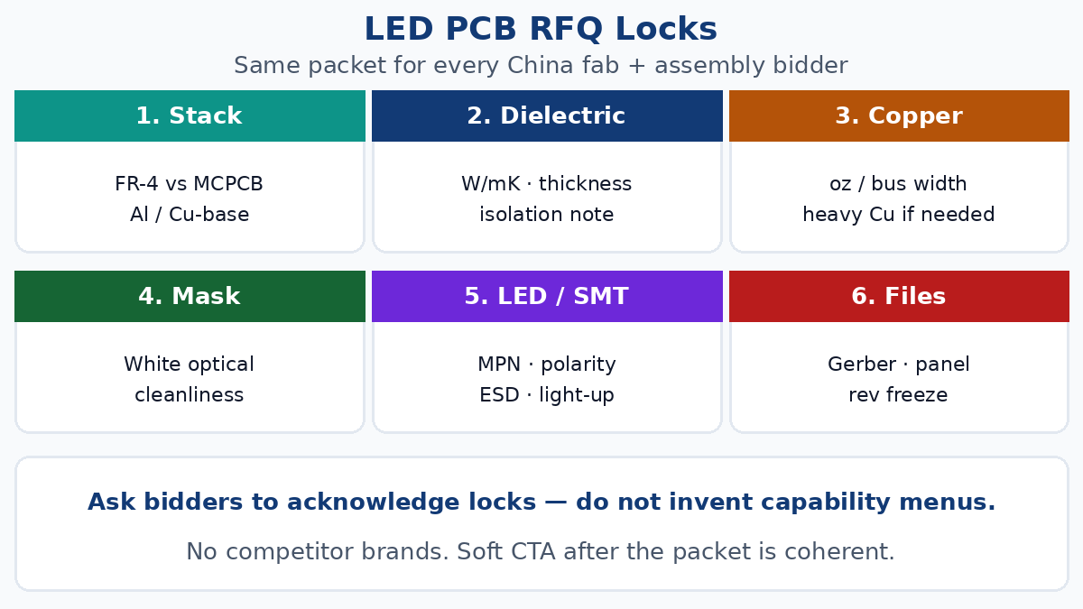
Copper, drive current, and array layout
Constant-current drivers stabilize brightness; resistor-only feeds belong on low-power indicators. On the board:
- Size traces and pours for continuous current plus margin, not only “fits between LEDs”
- Feed long strips or bars from both ends or at intervals when voltage drop would dim far LEDs
- Keep LED pitch consistent when optical uniformity matters; document binning / MPN so assembly does not mix bins silently
- Separate power and sense returns when the driver layout requires it — shared skinny returns cause flicker and EMI headaches
Array layout is optical and thermal at once. Dense packs raise local flux; sparse packs may need more copper area per watt. COB vs discrete packages change pad size, paste volume, and reflow mass. Lock the LED MPN (or approved alternates with equivalent thermal pad) before the fab freezes Gerbers.
White solder mask and reflectivity — without overselling
White mask is common on LED boards because it reflects light and helps lumen extraction and uniformity. That does not mean every white ink is optically equal, or that “white” alone guarantees lifetime reflectance.
Honest RFQ notes:
- Color and finish (matte/gloss) if optics care
- Cleanliness and no-silkscreen zones under lenses or secondary optics
- Awareness that heat and light can yellow some formulations over life — if optical maintenance matters, say so and ask process guidance; if the plate is a hidden driver board, standard mask may be enough and cheaper
- Pad openings and dams that do not contaminate LED lands
Do not invent reflectance percentages or “XFPCB optical white” grades on the cover sheet. Ask whether the shop’s white process matches your optical expectation; accept that a driver-only aluminum plate and a visible light-engine plate are different mask conversations.
Surface finish still matters for wetting and shelf life — ENIG, OSP, immersion tin, and other finishes each have process and storage tradeoffs. Match finish to LED pad size, assembly timeline, and any gold-finger or connector needs on the same panel. Name finish; do not leave it to the cheapest checkbox.
Panelization, outline, and long LED bars
LED products often want long, narrow boards or many identical light engines on one panel. Panelization mistakes show up as warpage, broken tabs, and pick-and-place mishandling.
Buyer locks:
- Outline tolerance, V-cut vs tab-route, and break-tab locations that do not stress LED rows
- Tooling holes and fiducials for SMT accuracy on dense arrays
- Warpage expectation for long bars (metal-core and FR-4 both warp if process and thickness fight the outline)
- Scoring or connectors between modular segments when field length varies
Send a panel drawing with the Gerbers when the array is non-trivial. “Panelize however you like” is how first articles arrive with LEDs near stress risers.
Assembly: polarity, ESD, and reflow notes
LED packages are polarity- and ESD-sensitive. Assembly notes that belong with turnkey PCB Assembly scope:
- Cathode/anode silkscreen or polarity marks that survive mask color; do not bury polarity only in a CAD attribute
- ESD handling class for the LED MPN and any driver ICs
- Moisture sensitivity and bake rules when the datasheet requires them
- Reflow profile awareness — metal-core plates have different thermal mass than FR-4 of the same outline; large COB packages need profile verification, not a generic “LED SMT” assumption
- Paste and aperture notes for thermal pads (coverage fraction, void concern if thermal criteria care)
- AOI / light-up / aging expectations if you buy functional screening — say sample vs 100%, and what “light-up” means (current, duration, pass/fail)
Pick-and-place rotation errors on LEDs are expensive: the board may power, but directionality or series string behavior is wrong. Fiducials, clear polarity marks, and a written first-article light-up check beat hoping AOI catches every cathode mark on white mask.
When fab and assembly are split, freeze the same revision of Gerber, centroid, and BOM across both. When they are combined, still put polarity, ESD, and reflow notes in the assembly package so the quote is not “SMT included” with zero LED process language.
China fab RFQ locks for LED PCB boards
Comparable quotes need the same sandwich and acceptance rules. Use Manufacturing Files discipline — Gerber (or ODB++), stack or MCPCB construction note, mechanical drawing, BOM/XY when assembled — and lock fields below so bidders are not inventing dielectric class.
| Field | Why it matters on LED boards |
|---|---|
| Construction | FR-4 multilayer vs single-sided MCPCB vs hybrid; layer count if FR-4 |
| Base metal / thickness | Aluminum (or copper-base) mm and alloy class when metal core |
| Dielectric | W/m·K class and thickness / isolation note for MCPCB |
| Copper weight | oz or µm; call heavy copper when current demands it |
| Solder mask | White (or other) + optical/cleanliness notes if lumen-facing |
| Surface finish | ENIG / OSP / etc. matched to pads and shelf life |
| Outline / panel | Contour, V-cut/route, tooling, warpage note for long bars |
| LED MPN / binning | Approved parts; no silent “same outline” substitutes |
| Thermal / TIM | Via or MCPCB path; TIM ownership on turnkey |
| Assembly | Polarity, ESD, reflow, AOI / light-up / aging sample plan |
| Qty / revision | Proto vs production band; frozen file rev |
| Test | E-test, dielectric sample if required, visual class |
Ask bidders to acknowledge those locks in writing. Do not invent XFPCB TAT tables, price lists, or certificate menus on the RFQ cover. Process capability answers come from DFM against your files — not from brochure copy pasted into the PO.
For schedule-sensitive first articles, say the revision freeze date and whether a quick-turn PCB lane is in scope as a schedule ask, not as a substitute for incomplete stack notes. Incomplete dielectric and copper fields still produce non-comparable quotes even on a rush PO.
Soft next step
An LED PCB board is a thermal, electrical, and optical contract on copper. Use FR-4 when power and enclosure already close the junction budget; move to aluminum (or other) metal core when the short path into metal is what lifetime needs. Put dielectric, copper weight, mask honesty, array panelization, and LED assembly polarity/ESD notes on the same RFQ that carries Gerbers. When the packet is coherent — stack intent, files, LED MPN, and acceptance — share it through How to Place an Order and let manufacturing engineering answer against the drawing. Soft CTA only: lock the path before lumen and lifetime arguments start in the field.