
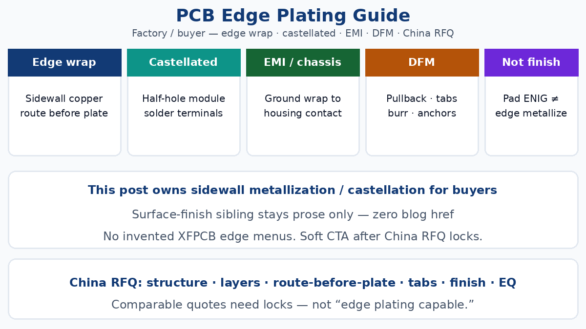
Edge plating is not a surface-finish choice with a different name. Buyers who write “gold edge” on an RFQ and mean ENIG on pads often get the wrong process. Sidewall metallization — also called side plating, edge wrap, or plated rout — deposits copper on selected outer edges or internal cutout walls so those walls connect to specified surface or internal copper. Castellated half-holes are a related but separate structure. This page owns the factory/buyer frame for PCB edge plating: when modules, EMI/chassis contact, or connectorless interconnect need a metalized edge; which DFM locks (route-before-plate, copper pullback, tab placement, burr control) keep China fabs quoting the same traveler; and what inspection actually fails before award. Ordinary pad finish selection — HASL, ENIG, OSP, Imm Ag/Sn, ENEPIG, hard gold — already lives on the pcb-surface-finish sibling lane. Name that lane in prose; do not clone or href it. Soft CTA only. No competitor brands. No invented XFPCB edge-plating capability menus, TAT claims, or $/edge premiums.
What edge plating is on a fab traveler
A plated edge is copper on a sidewall that was exposed by routing (or slotting) before metallization. After electroless seed and electrolytic build, the wall may receive the same solderable finish as the rest of the board, or a selective contact finish where the drawing calls for wear or enclosure contact. The electrical job is continuity from named layers to the wall — ground plane wrap for EMI/chassis contact, power/return tabs, or module-edge solder lands — not pad flatness for SMT paste.
Three structures get mixed in buyer English:
- Continuous or segmented edge plating — metalized outer perimeter or named edge segments
- Internal cutout / slot plating — metalized walls of a routed opening inside the board outline
- Castellated holes (half-holes) — plated through-holes cut open after plating to form discrete half-cylinder terminals for module soldering
Castellations are not “edge plating with holes.” They are PTH features that are broken open on final rout. Edge plating is a plated rout wall. Gold fingers are flat hard-gold contact pads on the board face — different again. Put the right name on the fab note so CAM does not invent a house default.
For multilayer builds, which layers touch the wall and which must pull back is a stack decision, not a finish decision. Keep layer-count and stack honesty on Multilayer PCB Guide and PCB Manufacturing conversations; this page only freezes the edge-metallization ask.
When buyers actually need a plated edge
Skip the brochure list. Score the award against jobs that change process sequence and quote risk:
Module interconnect without a connector. Castellated edges let a daughter card solder to a motherboard like a big SMT package. Discrete half-holes give inspectable fillets. Continuous edge wrap alone is a poor substitute when you need separate solder joints and visual FA per terminal.
EMI / chassis grounding. A metalized perimeter can give a low-impedance path from ground planes to a metal housing or shield can when solder-mask-free contact bands are defined. Edge plating does not by itself make the product EMC-compliant — plane strategy, stitching, connector returns, and enclosure contact still dominate. When the edge is part of an RF return or shield seam, treat the stack and return path with the same seriousness as an Impedance Control PCB RFQ: name the net, the contact band, and keep signal copper off the plated wall.
Connectorless edge contact / RF body ground. Edge-mounted RF connectors and some card-edge ground schemes want copper wrapping from reference planes onto the wall under the connector body. Keepouts around signal pads matter; plated ground must not bridge foreign nets.
Internal shielded openings. Plated slots or cutouts can form grounded walls inside the outline for cavities or mechanical features. Feasibility tracks slot width, corner radius, router access, and panel stability — ask before freezing CAD.
Heavy copper at the edge changes plating current density and peel risk; call copper weight honestly. Catalog Heavy Copper PCB language is process context, not a substitute for edge-specific pullback and tab notes on your drawing.
Route before plate — the sequence that cannot be vague
A sidewall cannot receive copper until it exists as an exposed wall. The correct traveler logic is:
- Fabricate and laminate the stack.
- Drill PTHs and other holes as required.
- Pre-route the plated contour or internal cutout while the board stays in panel on temporary tabs (plated rout).
- Clean the wall; electroless copper; electrolytic plate to thickness.
- Complete outer-layer pattern, solder mask, and surface finish.
- Final-rout only the support tabs — do not re-cut the functional plated wall.
If the fab routes the functional edge only after plating, the cutter shears finished copper and laminate instead of creating a metalized wall. That is not a cosmetic miss; it is the wrong process. Buyer English that says “plate the edge after outline” without pre-route language invites that failure mode.
Panel tabs interrupt plating where they sit. Full-perimeter plating usually still shows small unplated notches after tab removal. Partial plating can park tabs in unplated zones if the drawing allows it. Place tabs away from RF contact bands, connector bodies, and partial-plating transitions.
DFM that prevents award shock
Before the RFQ leaves your desk:
- Mark the plated contour on a mechanical / fab layer and on the fabrication drawing. For partial plating, dimension start/stop and permitted gaps.
- Name connected layers and nets. Copper that must wrap to the wall extends to the rout. Layers that must stay isolated pull back.
- Pull back unrelated copper. Signal traces, foreign planes, and pads need clearance that absorbs registration and outline tolerance — review every layer, not only the silkscreen outline.
- Anchor copper on outer layers near the wall so sidewall plating has something to tie to; weak anchors show up as peel during final rout or handling.
- Solder-mask policy on the contact band. Enclosure or chassis contact usually needs mask-free copper on the wall and adjacent lands. Mask-over-edge by accident kills contact.
- Connector and pad keepouts. Edge ground wrap must not short RF or digital signal pads.
- Castellation specifics when used. Hole size, pitch, unfinished half-hole cosmetics, and solderability criteria belong on the drawing — not a verbal “castellated OK.”
- Internal cutout geometry. Slot width, corner radius, and tool access must be manufacturable before you freeze EMI cavity art.
Attach Gerbers/ODB++, stack, and the mechanical callout through Manufacturing Files so “edge plate” is not a chat-side channel. Technical Capabilities pages describe house envelopes at catalog level; your drawing still has to name plated vs unplated segments and connected layers.
Full vs partial plating and castellation vs wrap
| Structure | What CAM sees | Typical buyer use | Main RFQ risk |
|---|---|---|---|
| Full edge plating | Most selected edges metalized; tabs leave local gaps | Perimeter ground / shield | Tab damage on functional wall |
| Partial edge plating | Dimensioned segments only | Local chassis or RF contact | Wrong start/stop; messy transitions |
| Castellated holes | PTH row cut to half-holes after plate | Module SMT interconnect | Hole size/pitch FA; ragged break |
| Via fence only | Discrete grounded vias near edge | RF field control without wall plate | Treated as if it replaced edge wrap |
A via fence and edge plating can coexist. One does not silently replace the other on the traveler. If you need both, list both.
Finish on a plated edge is not the edge decision
After the wall is copper, a finish protects it and sets solderability or contact behavior — ENIG for many solderable/contact edges, hard gold where repeated wear is real, other immersions when the house process and shelf plan allow. That choice is the same family decision as pad finish, applied to a sidewall. It is not a reason to merge this guide into the surface-finish buyer page.
Write two callouts when both matter: (1) edge metallization scope — layers, contour, castellation yes/no; (2) finish family on exposed copper including the wall. “Gold edge” alone still fails both.
Defects and inspection buyers should name
Common edge-plating FA themes:
- Incomplete sidewall coverage or thin spots from poor wall prep or plating distribution
- Copper lifting / peel from weak anchors or aggressive final rout into the plated wall
- Burrs and copper fragments from worn tools or bad feed — FOD risk at assembly
- Inner-layer shorts from insufficient pullback
- Exposed laminate at tab sites beyond drawing allowance
- Ragged partial-plating transitions when start/stop were not dimensioned
- Finish discontinuity on the wall when sidewall prep or finish compatibility was assumed
Inspection that matches the drawing usually includes visual sidewall coverage, continuity to the intended net, isolation from foreign nets, adhesion checks, burr/FOD review, outline dimensions, tab-removal condition, and microsection when the class or RFQ demands it. PCB board testing and inspection lanes own general electrical/test menus; here you only need to freeze edge-specific acceptance so first article does not argue about “how much unplated tab notch is OK.”
China fab RFQ locks for edge-plating awards
Export quotes diverge when the line item says only “edge plating” or “castellated.” Paste the same locks for every bidder:
- Structure class — continuous edge plate, partial segments, internal cutout plate, castellations, or combination — named per drawing layer.
- Connected layers and net — which copper wraps; which nets must stay clear; pullback intent on non-connected layers.
- Route-before-plate acknowledgment — bidder confirms plated-rout sequence; no silent post-plate outline shear of the functional wall.
- Tab policy — permitted tab locations, max unplated notch, keep-out from contact/RF zones.
- Finish on the wall — family named (and selective hard gold only where wear is real); no “gold” alone.
- Acceptance — continuity/isolation, visual class, burr criteria, first-article microsection if required.
- No silent swap — written EQ if the house changes castellation for wrap, drops internal cutout plate, or moves tabs into contact bands.
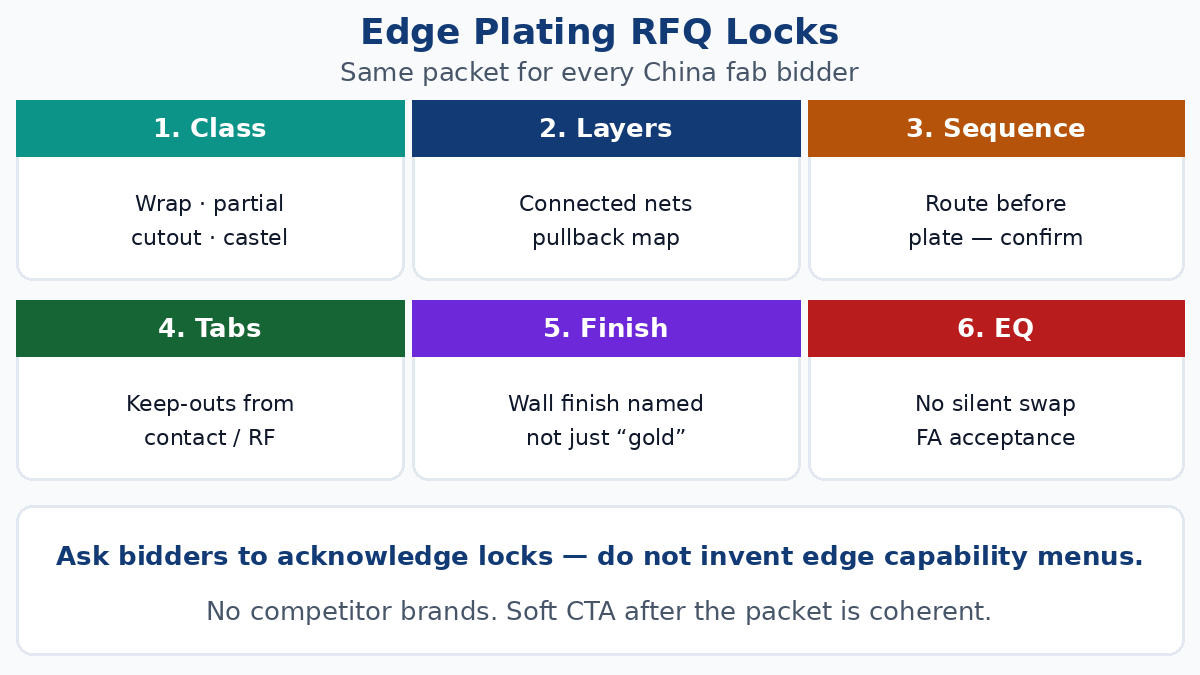
Comparable awards need those locks. “Edge plating capable” without structure class and connected-layer notes is not a comparable line.
Soft close
If your next China fab lot needs a metalized edge — module castellations, EMI/chassis wrap, or a plated cutout — freeze structure class, connected layers, tab policy, and wall finish on the drawing before you compare unit prices. When the packet is coherent, start from How to Place an Order and route Gerbers plus the fab drawing into quote. XFPCB will answer against the traveler you write, not against an invented edge-plating menu. The RFQ locks are the checklist.