
PCB board design that clears a China fab RFQ is not a prettier schematic screenshot. It is a controlled handoff: schematic and library freeze, placement and routing habits that survive etch and drill, then a release package whose stackup, impedance, drill map, finish, and copper weights match what CAM will build. Layout tutorials already cover return paths and place-then-route choreography. This note is the factory buyer path from schematic intent to fab-ready files — what must land in the package, which layout choices become scrap on the floor, and which RFQ gates stop quote churn.
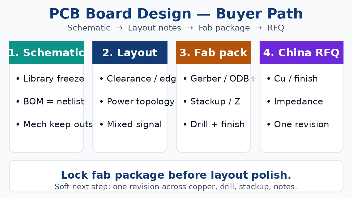
Schematic freeze before layout starts pricing
Buyers still open quotes while footprints, pin maps, and BOM lines disagree. Fab and assembly do not reconcile that for free.
Library and netlist locks. Footprints must match the exact datasheet land pattern, not a “similar package.” Pin-1 silk and copper must agree after any mirror or rotation. Export the netlist from the same schematic revision that owns the BOM. Thermal-pad vias on QFN and similar exposed pads belong in the library before place — open vias that suck paste into barrels are a first-article yield tax, not a CAM preference.
Mechanical and connector truth. Board outline, mounting holes, and connector keep-outs come from the enclosure and housing drawings. A through-hole connector footprint that omits mechanical keep-out is a layout bug that shows up as interference after Gerber, not as a helpful fab note.
Revision discipline. Refuse price comparison while BOM lines still say “TBD” for fine-pitch ICs. Assembly builds pick-place against the BOM; CAM builds copper against Gerber. Divergent revisions buy two wrong boards. Freeze library, BOM, and netlist, then open layout.
Schematic freeze is a buyer gate as much as an EE gate. Soft “we will clean the library later” language is how the first China RFQ already prices the wrong risk.
Placement and routing habits that survive fab (write them as RFQ notes)
Placement and routing advice is cheap until it becomes a traveler note CAM and buyers can check. Treat the habits below as release criteria, not blog slogans.
Place for etch, drill, and assembly access. Connectors and board-edge mechanicals first, then protection near the interfaces they guard, then hard packages (MCU, FPGA, RF, SERDES) where escape and continuous reference copper still exist, then power stages with short hot loops, then local decoupling, then glue logic and indicators. Zoning — noisy switchers away from quiet analog, intentional digital domains — is language both CAM and SMT understand. Leave AOI and rework access around dense parks; packing every park with LEDs is how inspection cost rises after the quote.
Clearance and edge. Stay above the fab’s published minimums for trace/space, pad-to-pad, and copper-to-outline — not at the absolute process floor. Edge clearance for copper and components protects panelization, routing (depaneling), and solder-mask alignment. Boards that “just fit” DRC at minimum often fail when CAM applies house rules or when V-score and tab-route eat margin.
Power topology as an RFQ note. Star distribution and daisy-chain distribution are not aesthetics. Star (or plane-fed local stars) keeps return and drop predictable for sensitive rails; long daisy chains of skinny necks under switching loads raise both voltage drop and EMI. Write current assumptions, copper weight, and plane versus trace intent on the stackup or fab notes so ampacity is not a silent house default.
Layer direction and reference. Agree stackup early enough that placement knows which layer is the unbroken reference under high-speed corridors. Adjacent signal layers typically run orthogonal so coupling stays manageable; layer swaps without nearby return vias open loops. A stackup decided after routing usually means return-path surgery and a second Gerber. Buyers should ask which layers carry controlled impedance and which planes are the reference before the layout is “done” — that answer belongs in the fab package, not in a post-quote email.
Mixed-signal split — intentional, not decorative. Separate analog and digital grounds only when the circuit needs it, then join at one intentional point. Accidental multi-point bridges defeat the split; routing quiet nets over noisy return gaps defeats it faster. Put the join strategy and any plane-cut keep-outs in fab notes when the design depends on them.
Avoid sharp 90° corners on etch-sensitive nets. Prefer 45° or gentle bends on fine lines where etch undercut and impedance matter. Decorative matching that crosses plane splits is worse than a short unmatched run over solid reference. Length-match only where the interface guide requires it.
These habits matter to fab because they change clearance, copper balance, via count, and impedance coupon need. Write the non-negotiables on the release notes; do not assume CAM invents them from a green DRC report.
What must land in the fab package
A fab-ready release is a revision-aligned set CAM can build without guessing. Pretty screenshots are not a package.
Gerber or ODB++ (one primary data set). Prefer a single agreed format. Mixing half-updated Gerbers with an old ODB++ dump is a classic hold. Include copper layers, solder mask, silkscreen, paste (if SMT will use the same archive), board outline, and any mechanical or keep-out layers the fab must honor. Name layers clearly; cryptic CAD defaults burn quote time.
Drill map and NC drill. Plated versus non-plated, finished hole sizes, and tolerance class when the design needs them. Blind/buried or back-drill callouts belong here with the stackup, not in a side email. Missing drill files or inch/metric mismatch still scrap first articles.
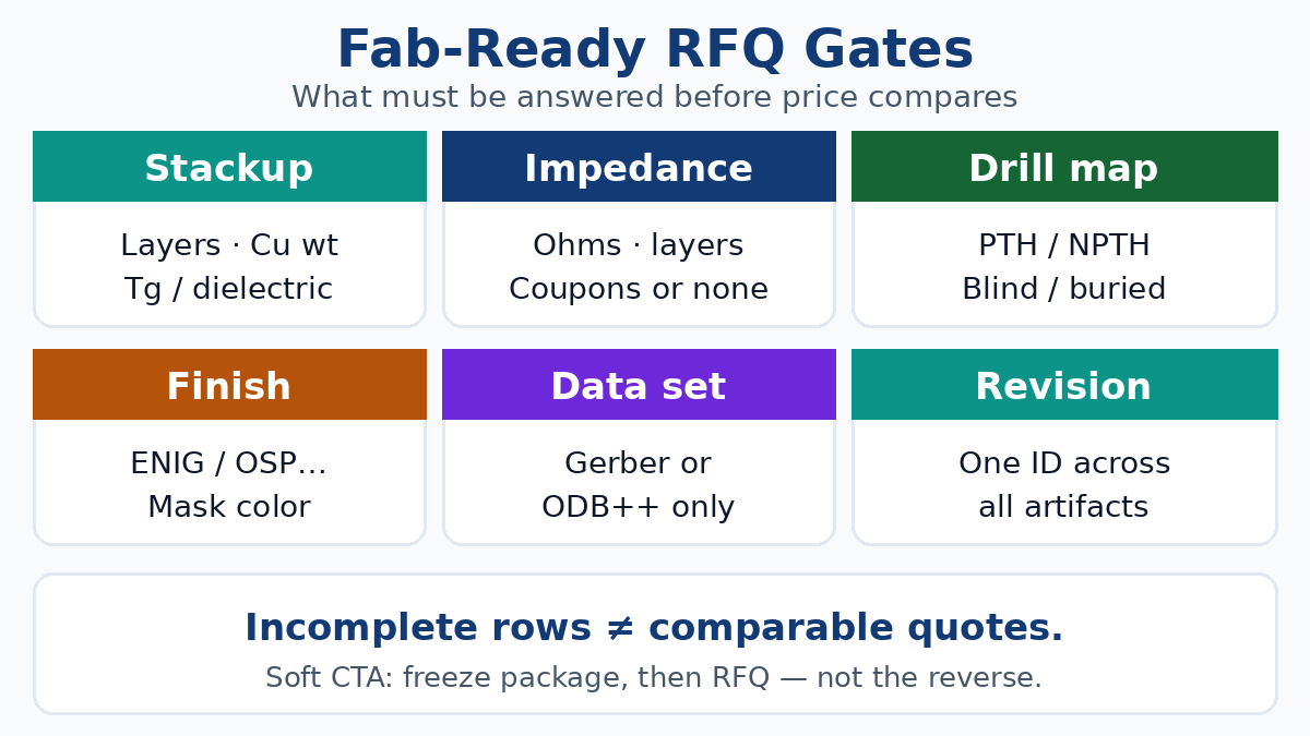
Stackup intent. Layer count, dielectric thickness windows, copper weights per layer (outer and inner), and material family or Tg when the design froze them. Soft “standard 4-layer FR-4” without copper and dielectric windows leaves CAM free to quote a house default that breaks impedance or ampacity assumptions.
Controlled impedance (when any). List target ohms, tolerance, which layers and nets or differential pairs, and reference plane. Ask for coupons and how results travel with the lot. Impedance without coupon language is a brochure word.
Finish and solder mask. Name the surface finish (ENIG, immersion silver, OSP, HASL, and so on) and any thickness or coplanarity notes assembly already assumes. Mask color and soldermask expansion habits matter for fine pitch; “suitable finish” is not a lock.
Copper weights and special constructions. Heavy copper, via fill, tented or open vias on thermal pads, and edge plating or castellations when used — call them on fab notes. Silent omission is how thermal pads arrive wrong.
Fab notes and drawing. Outline tolerance, fiducials for SMT if the same package feeds assembly, polarity marks, revision block, and any IPC class for bare-board acceptance you intend to buy. One revision string across Gerber, drill, stackup, and notes.
Procurement should refuse to open price comparison until these artifacts exist at one revision. Incomplete packages generate “clarify” loops that look like slow fab response when the release was never fab-ready.
Layout-to-fab scrap causes buyers still underprice
Most first-spin scrap is not mysterious process magic. It is missing locks.
Pad and outline mismatch. Footprint pads that do not match the part, or outline that does not match the enclosure, fail at assembly or fit — after you already paid for panels.
Copper-to-edge and mask registration. Copper or vias too close to the routed edge; mask openings that leave fine-pitch pads starved or bridged. Running at absolute minimum clearance without house-rule margin invites CAM EQ or silent scrap.
Annular ring and drill. Undersized pads for the finished hole, slot drills without correct callouts, or plated holes marked as NPTH. Hole-wall and ring failures show up in microsection or e-test, not in a schematic review.
Impedance and stackup drift. Design assumed one dielectric and copper weight; quote used another. Without stackup and coupon locks, the board can pass DRC and still fail SI.
Silkscreen and polarity. Pin-1 and diode polarity wrong or on copper; silkscreen into pads. Cheap to fix in CAD; expensive after stencil and parts.
Revision skew. Gerber rev A, BOM rev B, pick-place rev C. China fabs and CMS lines will build what you sent — not what you meant in chat. Hold one revision block across copper, drill, stackup PDF, and fab notes; archive the zip with that same ID in the filename so purchasing and CAM are looking at one artifact.
Unstated specials. Via-in-pad without fill callout, edge connectors without bevel or nickel/gold thickness, and castellations without drawing notes routinely become EQ holds or wrong process. If the CAD used a special, the fab package must name the process step.
Price the scrap causes as release checklist items. “We always catch that in CAM” is not a substitute for a complete package.
China fab RFQ checklist — gates that change the quote
Overseas buyers lose days when the RFQ omits gates every China fab CAM desk will eventually ask. Put them on the first ask.
- Quantity, panelization preference, and lead time class — prototype versus production framing changes process and price.
- Layer count, board size, thickness, and material / Tg — named when the design froze them; no silent “equivalent FR-4” if impedance or thermal depends on a family.
- Copper weights outer / inner — match ampacity and impedance assumptions.
- Surface finish and solder mask / legend colors — match assembly process (flatness, wire-bond, shelf life).
- Min trace/space, min hole, aspect ratio — confirm against fab capability; do not design at a capability you did not buy.
- Controlled impedance table + coupon expectation — or an explicit “no impedance control” line so CAM does not invent one.
- Drill file + plated vs NPTH map — including any blind/buried or back-drill.
- Specials — via fill, heavy copper, edge plate, castellation, gold fingers, impedance coupons travel rule.
- Acceptance — bare-board electrical test depth, IPC-6012 class if you require it, microsection or coupon report when risk warrants.
- Data package — Gerber or ODB++, fab drawing/notes, stackup, BOM if fab needs it for marking, single revision ID.
- Shipping and packing — moisture barrier, panel vs single, marking — when first article logistics matter.
- Contacts for EQ — named engineer for CAM questions so holds do not sit in a generic inbox.
When two plants return different prices, compare the answered checklist rows — not the headline number. A cheaper quote that assumed no impedance coupons, lighter copper, or a different finish is not the same board. Ask for capability confirmation on min hole and aspect ratio when your design sits near the edge of commodity multilayer process.
Reject replies that quote “standard multilayer” without answering copper, finish, impedance, and drill. Incomplete answers are not comparable prices.
Soft next step
Treat PCB board design as a buyer-controlled path: freeze schematic libraries and BOM, place and route with clearance, edge, mixed-signal, and power topology written as notes that survive fab, then release Gerber or ODB++ with stackup intent, impedance (or an explicit none), drill map, finish, and copper weights under one revision. Use the China fab RFQ checklist on the first ask so CAM questions arrive as confirmation, not as a redesign. Share the same revision package when you compare plants. Soft next step: lock the fab package before you chase layout polish that never reaches the traveler — that is how schematic intent becomes boards you can assemble without scrap theater.