
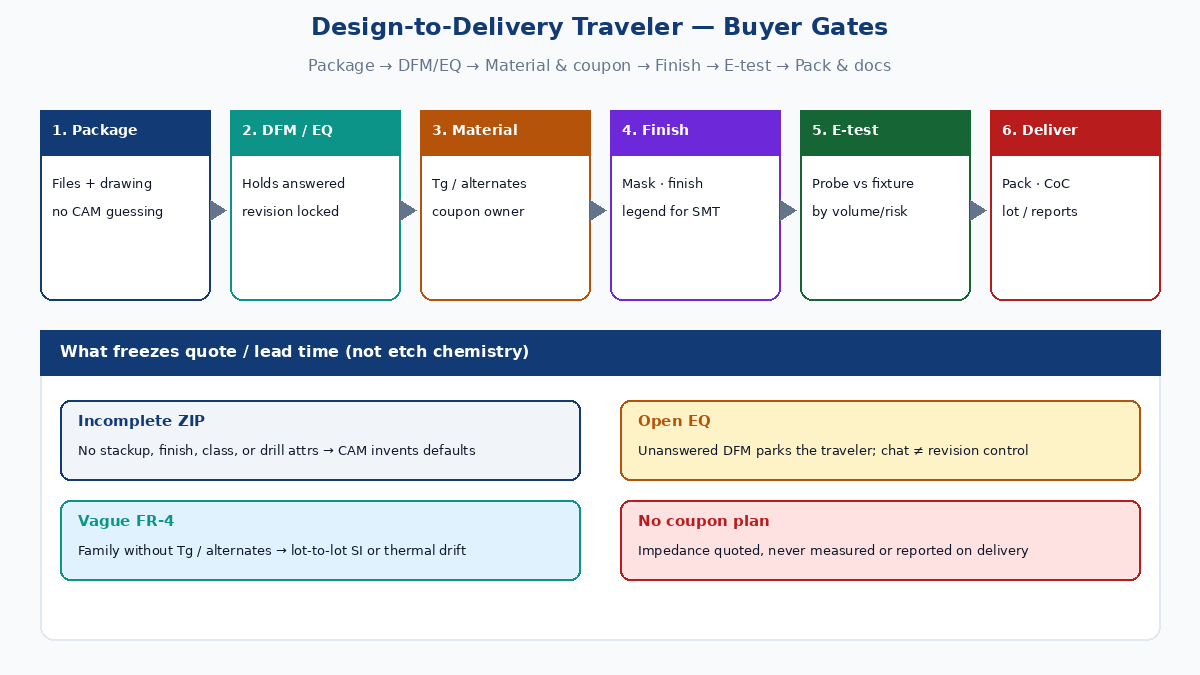
Overseas buyers often ask for "the PCB fabrication process from design to delivery" and get a chemistry brochure: photoresist, etch, laminate, drill, plate, mask, finish, test. That sequence is real — and it is not what freezes your quote or your ship date. What freezes them is the traveler: incomplete fab packages, unanswered engineering questions, material substitutions, impedance coupon ownership, finish choices that fight the assembler, and packing docs that do not match the PO.
This guide is for procurement and hardware leads sourcing bare boards from a China factory (or a China fab feeding overseas SMT). It walks the design-to-delivery workflow as a set of decision gates — what must be in the package before CAM, which DFM holds move cost and lead time, how China engineering questions and material callouts work on the traveler, finish/mask/legend as assembly-readiness choices, bare-board electrical test by volume, and the packing/traceability paperwork that closes the loop. It does not re-teach every plating bath. Confirm stackup, finish, class, and test notes on your drawing; brochure stage lists are not RFQ fields.
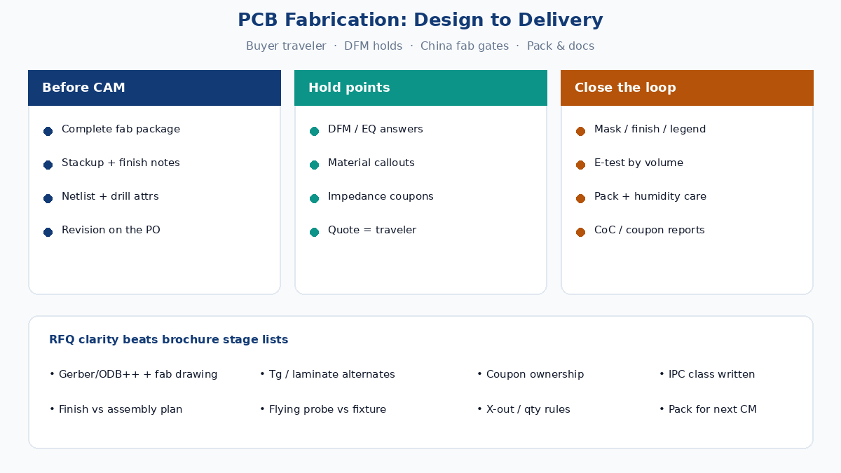
Gate 1 — Fab package that CAM can release without guessing
Fabrication does not start when panels enter the cleanroom. It starts when CAM can build a traveler without inventing missing notes. A schematic alone is not a fab package. A ZIP of copper layers with no stackup and no acceptance class is a delay waiting for an email thread.
Before you hit "send RFQ," the package should usually include:
- Gerber X2, ODB++, or IPC-2581 with consistent layer names (not "Layer1 / New Layer copy")
- NC drill with plated vs non-plated attributes clear
- Fab drawing — outline, thickness, copper weight per layer, solder-mask and legend color, surface finish, IPC acceptance class, special processes
- Stackup — cores, prepregs, dielectric targets, impedance table if controlled
- Netlist (IPC-D-356 or equivalent) when electrical test will use it
- Impedance / coupon notes — who owns coupon location, targets, and report format
- Material callouts — laminate family or approved alternates; do not leave "FR-4" alone if Tg, halogen-free, or low-loss matters
- Quantity, panelization preference, and delivery docs expected with the shipment
ODB++ and IPC-2581 reduce layer-name chaos versus classic Gerber sets, but they still need human fab notes. CAM will not quietly upgrade you to the laminate your RF engineer assumed, or to Class 3 plating, because the product "looks critical."
Procurement tip: If two vendors quote from the same ZIP and one price is dramatically lower, check which notes were treated as "TBD / standard." Cheap quotes often assume OSP, Class 2, no impedance report, and material brand flexibility you did not intend.
Gate 2 — DFM holds that change quote and lead time
DFM is not a courtesy. It is where the factory tells you the board as drawn cannot be built at the quoted yield, or cannot be built at all without a change. Treat DFM questions as schedule risk, not noise.
Holds that routinely move money or days:
- Trace/space and annular ring below the process window you were quoted — forces a process upgrade or layout change.
- Aspect ratio / drill size vs board thickness — microvia or sequential build may be required; that is not a free swap from through-hole.
- Copper imbalance and plane gaps that drive warp after lamination — may need copper thieving or stackup tweak.
- Solder-mask dams and openings that cannot hold at fine pitch — assembler will feel this as bridges later.
- Impedance targets without a manufacturable stackup — CAM proposes a stack; you approve dielectric and line width, or the quote was fiction.
- Finish vs pitch / multiple reflow — HASL may be wrong for fine BGA; ENIG cost and lead time differ from OSP.
- Panelization and scoring that break thin boards or leave ceramic caps near the outline unprotected.
When the factory sends engineering questions (EQ), answer with revision-controlled notes — not chat screenshots. Unanswered EQ parks the traveler. Partial answers ("use whatever FR-4 you have") create boards that pass fab AOI and fail SI or thermal life later.
Build a habit: same DFM checklist on every RFQ so vendor A and vendor B are priced against the same holds. Otherwise you are comparing optimism, not process.
Gate 3 — China factory traveler gates buyers actually feel
On a China fab floor the traveler is the contract the operators see. Buyers overseas feel three gates most often: engineering questions, material callouts, and impedance coupon ownership.
Engineering questions — CAM flags missing plated-hole attributes, unclear layer order, conflicting thickness notes, or silkscreen over pads. Fast teams reply inside one revision cycle with a marked PDF or updated ODB++. Slow teams lose a week while the panel slot slips to another job. Put a named technical contact on the PO, not only a purchasing inbox.
Material callouts — "FR-4" is a family, not a SKU. If you need high-Tg for lead-free assembly, halogen-free for a market requirement, or a specific Dk/Df for controlled impedance, write the family or approved alternates. Factories keep stock of common Tg FR-4; specialty laminates add purchase lead time and sometimes a minimum buy. Approving an alternate laminate mid-build without checking SI or Tg is how "same Gerber" boards behave differently lot to lot.
Impedance coupon ownership — Decide who places coupons (customer vs fab), where they sit on the panel, what TDR or coupon report you want, and whether coupons ship with the boards or stay at the factory. If the RFQ says "50 ohm single-ended" and nothing else, CAM will pick a stack that looks close and you may never see measured data. For RF and high-speed digital, coupon discipline is part of delivery — not an optional lab favor.
Also name revision control. China fabs will build Rev A forever if the PO still says Rev A. When layout changes mid-quote, update the file set and the PO revision in the same message.
Gate 4 — Mask, finish, and legend as assembly-readiness decisions
Solder mask, surface finish, and legend are often treated as cosmetics. For the assembler they are process inputs.
Solder mask — Color is secondary to opening accuracy, dam width, and via treatment (tented, plugged, capped). Mask that encroaches on fine-pitch pads forces hand touch-up or yield loss at SMT. Via-in-pad that needs fill/cap must be on the fab note; "we'll figure it out at assembly" usually means paste wicking and voids.
Surface finish — Choose for the assembly plan, not for a brochure preference:
- ENIG — flat, fine-pitch friendly, longer shelf life; cost and nickel/gold thickness notes matter for wire bond or harsh environments.
- OSP — low cost, short shelf / limited reflow cycles; good when boards go straight to SMT.
- Lead-free HASL — rugged and cheap for many through-hole / coarse-pitch jobs; coplanarity can hurt fine BGA.
- Immersion silver / tin — application-specific; watch shelf life and handling.
- Hard gold — edge connectors and wear surfaces, not a default for every pad.
If the board will see selective wave, double-sided reflow, or long warehouse time before assembly, write that on the RFQ. Finish mismatches show up as poor wetting weeks after fab FQC looked fine.
Legend (silkscreen) — Reference designators, polarity marks, and revision text that help SMT and field service. Overprinting pads, vias, or tight fiducials is a DFM fail. Traceability marks (date code, UL mark, customer PN) belong in the legend plan if you need them on the board — not only on the packing list.
Think of this gate as assembly readiness: the bare board should arrive ready for the paste and placement plan you already intend to run.
Gate 5 — Bare-board electrical test choices by volume
Electrical test confirms connectivity against the netlist before components are placed. It does not replace AOI, impedance coupons, or later FCT on the assembled product — but skipping it on dense multilayer boards is how opens and shorts reach the SMT line.
Practical volume choices:
- Flying probe — no dedicated fixture; slower per board; fits prototypes and low volume. Good when revisions change often.
- Fixture / bed-of-nails — higher NRE, faster cycle; pays off when the same revision runs at volume.
- Sample vs 100% — some low-risk 2-layer jobs quote sample e-test; dense HDI and impedance-controlled boards usually need 100% or a clearly stated AQL. Write the expectation; do not assume.
- Coupon / process tests — plating thickness, thermal stress, solderability samples — separate from netlist e-test; call them out when Class depth or customer audit requires them.
Match test depth to risk. A one-off maker board and a 12-layer backplane should not share the same "standard test" checkbox without reading the quote notes. Ask whether failed nets are repaired, scrapped, or reported — repair policy affects what you receive.
Gate 6 — Packing, traceability, and delivery docs that close the fab loop
A board that passes e-test can still fail the buyer if packing and paperwork are wrong. Closing design-to-delivery means the shipment matches the PO and the next process can start without a detective story.
Typical close-out items:
- Packing — vacuum bags with desiccant and humidity indicator for OSP and moisture-sensitive finishes; separators that do not scratch ENIG; panel vs single-board packing as ordered.
- Traceability — date codes, lot / panel IDs, traveler numbers that map to material lots when you need them for returns or audits.
- Documents — packing list tied to PO and revision; certificate of conformance if required; impedance or coupon reports if quoted; material certs when the RFQ asked for them.
- Quantity and X-outs — panel X-out rules and how partial panels are counted against the PO.
- Ship mode and Incoterms — who owns customs paperwork; whether boards can sit in a hot warehouse before SMT (finish shelf life).
If assembly is overseas or at a second China CM, align packing with that CM's incoming inspection. Boards dumped loose in a carton may pass fab FQC and arrive with bent corners or scratched pads.
How buyers should use this traveler (without buying a chemistry textbook)
You do not need to memorize etch chemistry to buy boards well. You need a package that CAM can release, a DFM loop that answers holds with revision control, explicit material and coupon ownership, finish/mask/legend chosen for the real assembly plan, e-test matched to volume and risk, and packing/docs that match the PO.
When those gates are written into the RFQ, China fab quotes become comparable, lead-time surprises drop, and the "from design to delivery" story stops being a brochure and starts being a schedule you can manage. Soft next step: put your next bare-board RFQ through this checklist once before you solicit price — then keep the same checklist for every vendor on the bid list.