
Precision sensor front ends and high-impedance amplifiers often fail in humidity chambers or after a “clean” no-clean reflow even when the SI model looks fine. The path that moves picoamps is rarely the controlled-impedance pair in an SI textbook — it is the surface between a sensitive node and a neighboring voltage: flux residue, moisture, ions under mask or conformal coat, a fingerprint across a sensor pad, or a pour that puts volts of ΔV next to a femtoamp input. This note is the layout + fab-note gate for overseas buyers and mixed-signal engineers RFQing a China fab or PCBA house: when leakage matters, SIR/contamination drivers, how guarding reduces ΔV, practical guard rings, package traps, coating interaction as process language, high-level return hygiene, the failure map buyers see, and RFQ fields that keep guarding alive. It is not a controlled-impedance primer, not an AI-server or 800G SI brief, and not a second cleaning-process article.
When surface leakage actually matters
Leakage budgets show up when the wanted signal current sits in the same order as (or below) the unwanted surface current. Typical pressure points:
- Photodiode, ion, or electrochemical sensor inputs with GΩ–TΩ bias networks.
- Precision instrumentation amplifiers, electrometer-style front ends, and charge amplifiers.
- Low-bias CMOS or JFET inputs where offset and drift specs assume picoamp or sub-picoamp input current.
- Sample-and-hold or integrator nodes that hold charge long enough for surface paths to look like “drift.”
- Mixed-signal boards where a digital rail or switching net sits next to a high-Z analog pad on the same outer layer.
- Products that must pass damp heat / humidity or condensation-prone field environments with the same offset they show in dry lab air.
If your front end is a 50 Ω RF path or a stiff digital bus, surface picoamps are usually irrelevant — spend layout time on impedance and EMI, not guard rings. Guarding earns money when a few volts of ΔV across a contaminated surface can move more current than your sensor produces.
💡 Buyer check: Get the allowed input leakage (or max ΔV under humidity). Without a number, “guarded high-Z” RFQs produce decorative rings CAM treats as ordinary copper.
What drives the surface path
Surface leakage is a parallel conductance across the board surface (and sometimes under mask or coat). SIR is the factory language for how insulating that path stays after process and aging. Common drivers China fabs and PCBA lines see:
| Driver | What happens on the board | Why high-Z cares |
|---|---|---|
| Flux / process residue | Ionic or hygroscopic film between pads after reflow or hand touch-up | Conductance rises with humidity; “dry bench OK, chamber fail” |
| Humidity / absorbed moisture | Water film or absorbed H₂O lowers surface resistivity | Seasonal and damp-heat fails without schematic change |
| Fingerprints / handling | Skin oils and salts bridge keepouts | Prototype boards “mysteriously” worse after fixture handling |
| Under-mask contamination | Residue trapped under solder mask at pad edges | Looks clean optically; still leaks under bias + humidity |
| Under-coat / coat voids | Conformal coat over dirty board, or pinholes / incomplete coverage | Coat can seal in ions or leave leakage corridors |
| Closely spaced high ΔV copper | Guard missing; pour or via farm next to protected node | Geometry sets the voltage that drives whatever conductance exists |
| Improper solder-mask openings | Mask dams or openings that leave residue lakes or thin creepage | Creepage and cleaning access both suffer |
SIR and ROSE/ionic tests are process evidence, not a layout substitute. A coupon SIR pass can still fail at a sensor pin against a 3.3 V net with no guard and no-clean residue the coat never isolated. Do not invent numeric SIR limits unless the OEM standard requires them — write cleanliness class intent and confirm acceptance with the fab/PCBA before FA.
Physics in plain words — reduce the ΔV that drives leakage
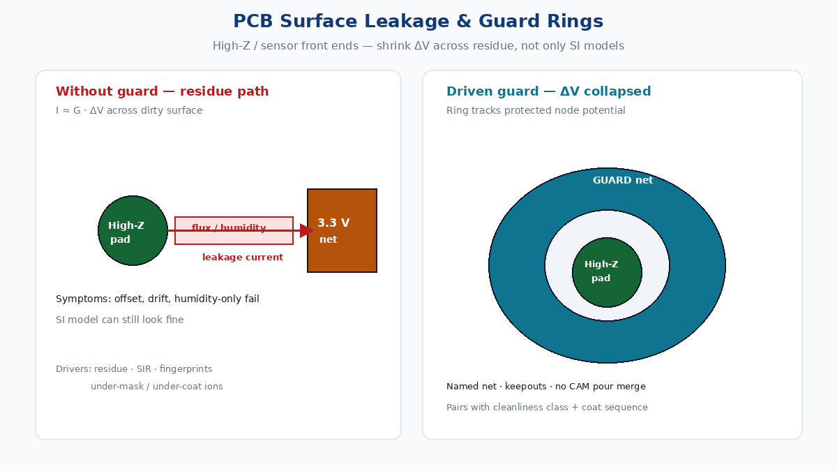
Ohm’s law still applies at picoamps. If a surface film has conductance G between two nodes, leakage current is roughly I ≈ G · ΔV. You cannot always drive G to zero on a production board that must survive reflow, handling, and humidity. You can shrink ΔV around the protected node.
That is the job of a guard: surround the sensitive copper with a conductor at nearly the same potential so the lateral field across the dirty surface collapses. With ΔV near zero, leakage collapses even when G is imperfect.
- Driven guard — buffer or dedicated driver forces the ring to track the node. Use when the node voltage moves.
- Grounded guard — ring tied to a quiet analog reference. Fine when the node sits near that reference; a grounded ring next to a node at 2 V still leaves ΔV to ground. Match guard potential to the node, not to a blanket “ground everything” rule.
Guarding does not replace cleanliness or coat discipline. Buyers who skip wash/coat notes and “fix it with copper rings” still ship humidity-only fails.
Guard rings that survive CAM and assembly
Implementation details decide whether guarding is real or decorative:
Layers. Start with outer-layer rings around the pad and short fanout. On multilayers, continue under the protected via when vertical leakage or via-to-pour coupling matters — a top guard with a hot pour on L2 under the via is a common miss. Clearances and mask rules are confirm-with-fab for your stack and copper weight.
Driven vs grounded. Driven guards need a named net (e.g. GUARD_SENS0) from the buffer pin, not a pour CAM will merge into GND. Grounded rings need an explicit quiet-reference tie — not “any ground via,” which may be a bouncing digital return.
Keepouts. Keep foreign nets, vias, and testpoints out of the island. Stitching vias that bring noisy planes up next to the pad defeat the ring. Component overhang that forces paste/flux into the keepout belongs on assembly notes, not only CAD.
Solder mask. Align openings or mask dams with the cleanliness path you bought (no-clean vs wash). Opening everything “to clean better” without a process note just invites fingerprints; sealing everything under mask can trap residue at the pad edge.
Net naming. List guard nets, driven vs grounded, and ban “helpful” CAM merges into chassis or digital GND. Silent pour merges are a classic NPI surprise.
Package and adjacent-pin traps
The PCB ring is useless if the package already leaks or couples next door:
- Adjacent pins on a fine-pitch package — a digital output or supply next to a femtoamp input — can dominate board leakage. Prefer packages with a dedicated guard pin, or leave unused pins as driven/grounded guards per the IC datasheet.
- Leadframe and mold-compound surface paths inside the package are not something the fab can fix with SIR coupons. If the IC is the limit, layout only stops making it worse.
- Via-in-pad or via farms under the body that connect to unrelated nets create vertical shortcuts.
- Probe pads and bed-of-nails targets that land on the protected island for “easy debug” become permanent leakage and ESD antennas in the field — move them outside the guard or gate them with series resistance the design can afford.
- Connector pins that bring dirty harness voltage next to the sensor input need the same ΔV thinking: guard, spacing, and sometimes a clean-side / dirty-side split on the connector.
Use the IC application note’s guard pinout before inventing a ring that fights the package.
Fab and assembly notes — make guarding survive the factory
Guarding is a layout + process pair. RFQs that only say “high impedance design” get ordinary travelers. Language that works:
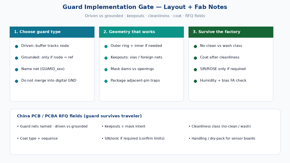
Cleanliness intent. State no-clean vs wash (name the process class). If high-Z nodes cannot tolerate typical no-clean residue under humidity, say so — do not assume wash because the schematic looks “analog.” Point to ionic acceptance as a process note, not a second cleaning SOP; your cleanliness document owns the recipe, this RFQ selects class and any ROSE/SIR evidence.
Coating sequence. If coat is required: type family (acrylic / urethane / silicone — confirm-with-fab), coverage map, and coat after cleanliness acceptance. Coating over active ions locks a leakage path under a nice film. Call keepouts at connectors/testpoints.
SIR / ROSE if required. Only when the end customer demands it. Name method family and sample plan; confirm limits with the fab. Prefer coupons that represent the guarded island geometry, not only a generic panel-rail pattern.
Mask, finish, handling. Finish choice does not erase ionic films. Dry-pack and handling notes matter — fingerprints on a photodiode pad are real scrap.
Guard net callouts. List names, driven vs grounded, and “do not merge into GND/chassis.” Attach a highlighted Gerber if CAM merges pours aggressively.
RFQ checklist (short)
- High-Z / guarded nets named; driven vs grounded stated.
- Keepouts and mask intent around guarded pads.
- Cleanliness class: no-clean vs wash (reference your process standard, don’t rewrite it).
- Conformal coat: yes/no, type family, sequence after cleanliness, coverage map.
- SIR/ROSE or ionic acceptance only if required — method + confirm-with-fab limits.
- Handling / dry-pack notes for sensor and front-end boards.
- Package pinout / unused-pin guard intent if the IC datasheet requires it.
- First-article electrical check under humidity or damp bias if that is the field risk — dry functional test alone misses the failure mode.
Failure map buyers see
| Symptom | Likely surface / process story | What to check |
|---|---|---|
| DC offset that grows with humidity | Surface G rises; ΔV across residue to a nearby rail | Guard presence/potential, residue class, coat voids |
| Slow drift / integrator walk | Charge leak off hold node | Guard on hold net, adjacent pins, probe pads |
| Dry bench pass, damp-heat fail | Hygroscopic film or incomplete coat | Cleanliness class, SIR evidence, coat sequence |
| Unit-to-unit scatter after assembly | Handling fingerprints, wash inconsistency | Traveler notes, glove/handling, FA on worst units |
| Guard “ring” still leaks | Ring merged to wrong net, or grounded while node is hot | Netlist vs Gerber pour, driven buffer connection |
| Coat looks fine, still fails | Ions under coat or pinholes at pad edge | Clean-before-coat evidence, coverage microsection |
When FA starts, ask for photos of the guarded island after coat, ionic/ROSE data if contracted, and a humidity retest with bias applied to the neighboring nets — not only a dry continuity pass.
Mixed-signal return hygiene (high level)
Guarding is not a full SI tutorial, but return-path mistakes recreate ΔV on the surface you just guarded. Keep digital return currents off the analog reference the guard ties to. Bridge analog/digital grounds at one defined point when the architecture requires it; do not lace stitching vias through the guarded island “for EMI.” Treat switchers and crystal drive as aggressors — spacing and return planning beat another copper ring. This post adds the surface ΔV lens to existing impedance and amplifier-layout practice; it is not a stack-up rewrite for a photodiode pad.
Closing
High-Z and sensor boards fail from surface conductance × voltage, not from missing an SI buzzword. Shrink ΔV with driven or correctly referenced guards, keep foreign copper out of the island, and pair guarding with cleanliness class, coat sequence, and optional SIR/ionic evidence on the China RFQ. Guard net names and process intent beat brochure phrases. Confirm clearances, coat chemistry, and cleanliness limits with the fab — then validate first articles under the humidity and bias the field will apply.