
Industry primers that list RoHS restricted substances, semiconductor GHG partnerships, additive “printed PCB” futures, and copper/tin recycling — then close with “partner with a sustainable, aerospace-quality, RoHS-certified house” — still leave overseas buyers awarding China fab and PCBA lots without substance and process gates written on the RFQ. Treat those industry overviews as outside orientation, not XFPCB plant awards. This page owns a different frame: a practical buyer guide to PCBs and the environment — RoHS / REACH as RFQ gates (not wall logos), what “lead-free” actually changes in fab and assembly, waste / chemistry handling questions to ask a China fab, recycling claims versus what a buyer can verify, and additive / printed PCB as a niche path, not a universal substitute for etched multilayer work. Soft CTA only. Sibling XFPCB lanes already own supply-risk buffers on the live supply-chain issues post, RoHS as one cell in the certification map on certified PCB suppliers, process depth on Lead-Free Assembly, and buy execution on Component Sourcing — link the service pages; do not clone the blogs. Later Batch5 insulating-materials / flexible-sensors guides stay separate — do not merge. Do not invent XFPCB as a “sustainable certified aerospace-quality” plant, and do not invent green awards or AS9100 / EPA trophies here.
What “environment” should mean on a buyer RFQ
For an overseas buyer placing bare boards or turnkey PCBA with a China fab, “PCBs and the environment” is not a climate essay. It is a set of substance, process, and evidence questions that either appear as explicit RFQ lines or show up as quiet compliance gaps after PO:
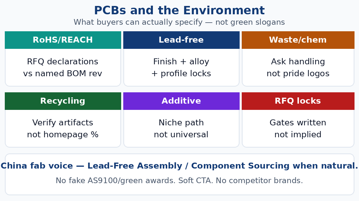
- RoHS / REACH as market-access gates — restricted substances, declarations against your finish / alloy / BOM revision, and REACH SVHC communication when your market requires it.
- Lead-free process deltas — higher reflow peaks, finish / alloy locks, moisture and void risk — not a homepage badge that replaces traveler notes.
- Waste and chemistry handling — etch / plate / strip / finish baths and sludge / wastewater questions you can ask without pretending to audit every EPA citation from afar.
- Recycling claims vs buyer verify — copper / tin recovery stories versus lot-level evidence a purchasing team can actually attach to a PO.
- Additive / printed PCB — low-waste niche for specific constructions; not a drop-in for conventional multilayer PCB Manufacturing volumes.
Capability depth that is not this essay lives elsewhere: certification evidence map on the certified-suppliers lane, supply calendar buffers on the supply-chain lane, and assembly process notes on Lead-Free Assembly. This guide stays on buyer-specifiable environment language.
RoHS and REACH — RFQ gates, not pride logos
RoHS restricts certain hazardous substances (commonly framed around lead, cadmium, mercury, hexavalent chromium, and related restricted phthalates under the regimes your market enforces) in electrical / electronic equipment destined for markets that enforce it. REACH adds EU chemical registration, evaluation, and communication duties — including SVHC awareness — that show up as declarations and material communication, not as a substitute for solderability or reliability testing.
Buyer failure mode: accepting a homepage “RoHS Certified” badge as if it already wrote your finish, solder alloy, and BOM revision into the lot file.
Useful RFQ paste (write your own numbers; do not invent XFPCB certificate IDs here):
- Declaration scope — RoHS conformity against named surface finish, solder alloy family, and BOM revision — not a generic plant statement.
- Exemption handling — if any RoHS exemption is claimed, name the exemption and the parts it covers; silent “mostly lead-free” is not comparable.
- REACH / SVHC response — when your customer or market requires it, ask for SVHC communication against the same revision; do not treat a RoHS PDF as automatic REACH closure.
- Kit substitution rules — for turnkey buys, lock authorized-channel / AVL rules via Component Sourcing so a broker “RoHS OK” part does not silently enter the traveler.
- Certificate vs product — plant ISO / quality certificates do not replace substance declarations (see the certified-suppliers lane for the broader map — keep this page on substance gates).
Route award logistics through How to Place an Order only after substance gates are frozen — not after a soft “we are RoHS” reopens the traveler post-PO.
What “lead-free” changes in fab and assembly
“Lead-free” is a process and materials lock, not a marketing synonym for “green plant.”
Bare-board side. Surface finish choice (ENIG, OSP, Immersion Tin / Silver, lead-free HASL where offered, and others) must match the reflow / wave plan and shelf-life assumptions. Fab notes that say “lead-free compatible finish” without naming the finish are not award-ready. Lock finish on the traveler beside stack and copper weight; pull depth from Technical Capabilities when you need process windows, not slogans.
Assembly side. Lead-free solder alloys typically run higher peak temperatures than tin-lead. That changes:
- Reflow / wave profile windows and peak limits on the traveler.
- Moisture sensitivity and baking rules for MSDs.
- Void / wetting risk on BGAs and fine-pitch when profiles drift.
- Rework heat budgets and how many thermal cycles a board may see.
Buyer practice: write alloy family, peak profile notes, and finish explicitly, then use Lead-Free Assembly for process-path language — do not duplicate that page’s depth here. Do not invent XFPCB “aerospace lead-free certification” claims; ask for process notes and lot evidence against the revision you order.
**What lead-free does not buy:** automatic RoHS lot evidence for every substituted component, automatic REACH closure, or immunity from poor waste handling at the fab. Substance declarations and process locks stay separate lines.
Waste and chemistry — questions to ask a China fab
PCB fabrication uses etch, plate, strip, mask, and surface-finish chemistries. Industry primers correctly note that unmanaged waste can be hazardous. An overseas buyer rarely runs a full environmental audit from a spreadsheet — but you can ask concrete handling questions that separate serious plants from brochure language:
- Which process chemistries does this construction use (etch / plate / finish family), and are any specialty baths required beyond the fab’s standard FR4-family window?
- Waste streams — how are spent etch / strip / plating baths and sludge handled (on-site treatment, licensed transfer)? Ask for the type of control, not a recycled slogan.
- Wastewater — is copper-bearing rinse water treated before discharge under the plant’s local permits? Buyers cannot invent permit numbers; they can ask whether copper recovery / treatment is part of the normal flow for the line that will run your lot.
- Hold points — what happens if a chemistry excursion hits a lot (strip / rework / scrap)? Environment language that ignores scrap rate still hits your schedule and cost.
Honest China fab voice: capable export houses routinely operate etch / plate lines under local environmental permits and ISO 9001-style plant systems. That is not the same as inventing XFPCB EPA awards, AS9100 green badges, or “zero-waste aerospace” marketing. Prefer written process + handling answers over pride logos.
When the construction leaves commodity FR4-family into HF, flex, aluminum / MCPCB, or heavy selective plating, ask which chemistry deltas apply — PCB Manufacturing product paths change baths and scrap profiles even when RoHS substance limits stay the same.
Recycling claims vs what buyers can verify
Copper and tin can be recovered from etch / strip streams and from end-of-life electronics. That industry fact is real. Buyer failure mode: treating a homepage “we recycle copper and tin” line as lot-level evidence for your PO.
What a purchasing team can usually verify:
| Claim type | Buyer-verifiable artifact | What it does not prove |
|---|---|---|
| RoHS / REACH declaration | Declaration vs named finish / alloy / BOM rev | Plant “green” awards |
| Lead-free process notes | Alloy + profile + finish on traveler | End-of-life recycling rate |
| Copper recovery at fab | Plant statement on etch / wastewater copper recovery practice | Your board’s recycled-content % |
| End-of-life PCB recycling | Downstream recycler / WEEE-path language from your region | That the fab already closed your product’s EOL |
Buyer practice: separate substance conformity for the lot you buy from circular-economy storytelling. If your customer requires recycled-content or take-back language, write that as a customer-driven requirement with named evidence — do not invent XFPCB recycled-content percentages or green medals.
Additive / printed PCB — niche, not universal
Additive and printed electronics approaches (including printed traces on selected substrates) can reduce subtractive copper waste for specific constructions — often simpler interconnects, sensors, or low-layer experimental builds. That niche is real and worth knowing.
What additive / printed is not:
- A universal replacement for conventional multilayer etched boards with controlled impedance, HDI, or high layer counts.
- An automatic RoHS / REACH shortcut — ink / paste chemistries still need substance gates.
- A reason to skip Manufacturing Files discipline (stack, finish, test) when you do use conventional fab.
Buyer practice: if a design truly fits additive / printed, treat it as a separate process path with its own materials, test, and volume limits. For the great majority of export China fab RFQs — FR4-family multilayers, flex / rigid-flex, aluminum / MCPCB, selective HF — stay on conventional PCB Manufacturing travelers and write environment gates as substance + process + handling questions above. Do not let an industry “printed PCB future” paragraph substitute for finish / alloy / declaration locks on today’s PO.
RFQ clauses that lock environment gates (paste-ready)
Export quotes diverge when environment language stays soft (“RoHS compliant,” “eco-friendly process,” “recyclable materials”). Paste comparable callouts:
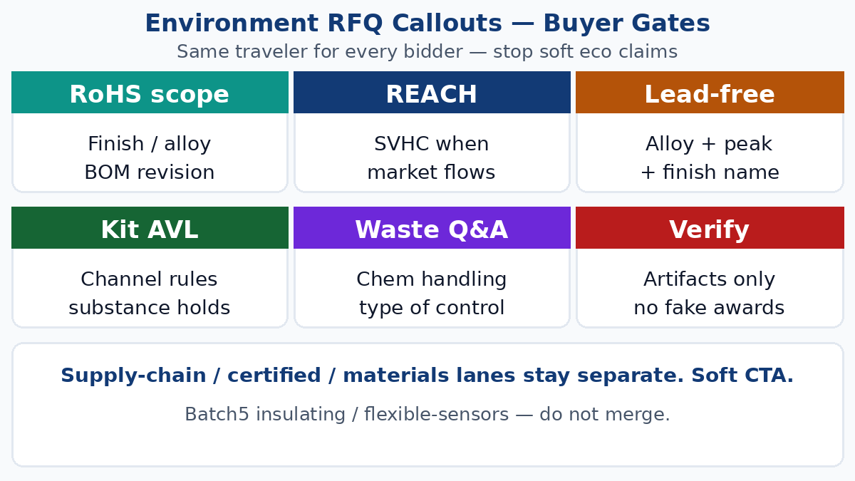
- RoHS declaration — against named surface finish, solder alloy family, and BOM revision; list exemptions if any.
- REACH / SVHC — response required when your market / customer flows it; same revision.
- Lead-free process lock — alloy family, peak profile notes, finish name; point process depth to Lead-Free Assembly without soft “lead-free capable” alone.
- Finish / material freeze — no silent finish swap or halogen-free / substance-relevant material swap without PE EQ.
- Kit AVL / channel rules — Component Sourcing substitution rules so substance evidence survives the kit.
- Chemistry / waste handling Q&A — brief written answers on etch / plate / finish waste and copper-bearing wastewater practice for the line that will run the lot — type of control, not invented award names.
- Recycling claims scoped — plant copper-recovery practice vs end-of-life take-back vs recycled-content % — only the scopes you actually need, with artifacts.
- No invented plant trophies — no XFPCB “sustainable aerospace-quality” invent, no fake AS9100 / green awards, no competitor brand ads.
China fab honesty — what environment language can and cannot buy
China export fabs routinely run lead-free finishes, RoHS-oriented declarations for EU / other market-access paths, and etch / plate lines under local environmental controls. That does not mean every homepage recycling paragraph, every additive demo, or every “green certified” collage is lot evidence for your traveler.
Honest buyer practice:
- Prefer declarations against your revision over plant pride logos.
- Prefer named finish + alloy + profile over “lead-free capable.”
- Prefer handling questions with written answers over invented EPA / AS9100 green medals.
- Keep supply-calendar buffers on the supply-chain lane; keep the full certification map on the certified-suppliers lane; keep dielectric / insulating deep dives for later Batch5 — do not merge.
Soft next step
Write RoHS / REACH declaration scope, lead-free finish / alloy / profile locks, kit AVL rules, and the waste / chemistry questions you actually need so every bidder answers the same traveler. Soft next step when substance and process gates are clear: send the RFQ through your normal path via How to Place an Order with manufacturing files attached — and pull Lead-Free Assembly or Component Sourcing language only when process or kit is on the critical path, not when a soft “eco-friendly” line was really an unlocked declaration.