
Overseas buyers awarding China SMT often discover solder bridges the hard way: a short on fine-pitch pins after first power-up, a lot held at AOI, or a rework invoice that was never priced into the RFQ. Sibling XFPCB lanes already own AOI depth, the broader QA-test suite, testing-methods overviews, SMT benefits, SMT vs through-hole tradeoffs, and solder-mask color choices — name those lanes in prose; do not clone them. This page owns a factory / buyer job: what a solder bridge is, design vs process root causes (pad spacing, mask dams, stencil aperture and paste volume, placement force, stencil cleanliness), prevention gates you can write into RFQ and DFM, how China SMT lines catch bridges (SPI → AOI → selective X-ray for hidden joints), and rework reality without inventing plant yield percentages. Soft CTA only. No competitor brands. No invented XFPCB defect rates or IPC awards.
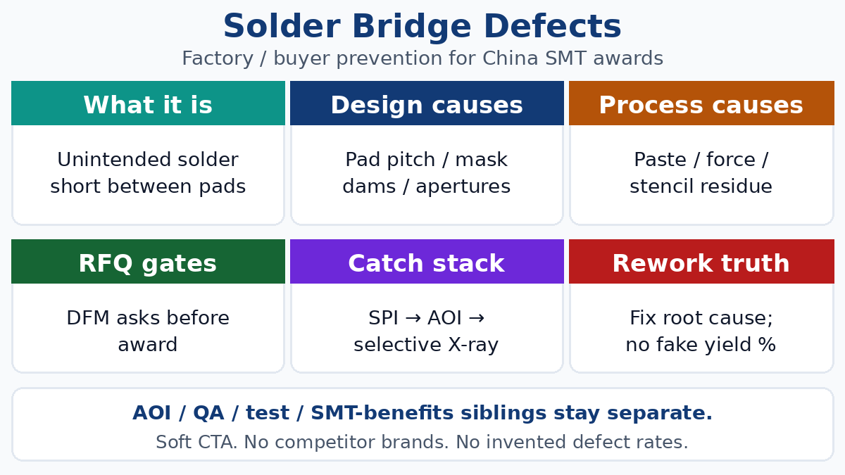
What a solder bridge is (and why it matters on export lots)
A solder bridge is an unintended conductive path of solder between two pads, pins, or traces that should stay electrically isolated. On dense SMT footprints — QFN, QFP, fine-pitch connectors, 0402 and smaller passives packed tight — the gap that should stay open is small, so excess paste, poor mask dams, or placement squeeze can close it in one reflow cycle.
Buyers care because bridges are shorts, not cosmetic blemishes. A single bridge can kill a board at first power, create intermittent field failures under thermal stress, or force 100% visual / optical holds that blow schedule. Unlike some opens that fail cleanly at ICT or flying probe, a bridge may pass a soft visual glance and still short two nets that only collide under load. Catching bridges early — before box build — is cheaper than discovering them in system test.
This guide stays on bridges as a defect class. Broader AOI pedagogy, full QA matrices, and end-to-end test-method catalogs live on their own posts; keep those lanes separate.
Design root causes buyers can still influence
Many bridges start on the CAD side long before a Shenzhen stencil hits paste. Designers chasing miniaturization shrink pad-to-pad and pin-to-pin clearance until the process window disappears. Buyers awarding SMT PCB Assembly should treat the following as RFQ / DFM conversation topics, not after-the-fact blame.
Pad spacing and pitch
When copper pads sit closer than the house’s proven paste and reflow window, bridges become statistical, not accidental. Ask for the plant’s minimum recommended pad-to-pad and pin pitch for the package families on your BOM — especially fine-pitch ICs and connectors. If your layout is inside their comfort band, write that assumption into the DFM reply so “we can run it” is not a silent stretch.
Solder-mask dams
Mask dams between adjacent pads are a primary physical barrier against paste smear and reflow wetting across the gap. Missing or undersized dams between fine-pitch pins are a classic bridge setup. Solder-mask color can help human contrast on inspection benches — that color conversation already has its own page — but color does not replace a real dam. Ask CAM whether mask dams exist between critical pin pairs and whether the mask opening / pad relationship follows the house process (SMD vs NSMD as applicable).
Stencil aperture and paste volume (design-adjacent)
Aperture design is often owned jointly by the fab’s assembly engineering and the customer’s DFM. Oversized apertures dump excess paste; poorly shaped apertures leave paste where it can smear toward neighbors. On dense areas, ask for aperture reduction rules, home-plate or window-pane shapes where appropriate, and whether paste volume was simulated or historically proven on similar pitch. Do not assume Gerber paste layers equal a production stencil without a process engineer’s eye.
Through-hole and mixed technology notes
Bridges are most discussed on SMT, but wave or selective solder on Through-Hole Assembly can also bridge between leads when hole-to-hole pitch, pallet design, or flux volume is wrong. Mixed SMT + TH assemblies need both process windows named on the traveler — not a single “assembly quality” checkbox.
Process root causes on the SMT line
Even a clean layout can bridge when paste print, placement, or stencil hygiene drifts. These are the process knobs China SMT lines tune daily — and the ones buyers should hear about in EQ replies, not only in marketing slogans.
Paste volume and print pressure
Too much paste is a direct path to bridges. Print pressure, snap-off, and squeegee wear change deposited volume. SPI (solder paste inspection) after print is the first quantitative gate: volume, height, and area against limits. If a quote never mentions SPI on fine-pitch work, ask how excess paste is caught before reflow.
Placement force and alignment
Pick-and-place nozzles that press too hard can squeeze paste sideways off the pad. Misalignment puts a component so that paste from one pad reaches toward its neighbor under reflow wetting. Ask how placement force is set for fine-pitch packages and whether first-article optical checks include bridge-prone pin fields.
Stencil cleanliness and residue
Residue left in apertures or on the stencil underside changes the next print. Dirty stencils create irregular paste deposits that look random until someone notices a repeating bridge pattern on the same pins. Cleaning cadence, underside wipe, and inspection of stencil condition belong in process control — not only in a “we clean regularly” sentence.
Preheat and reflow profile
Insufficient preheat or a profile that drives aggressive wetting without controlled time-above-liquidus can worsen bridging on already-marginal paste deposits. Profile ownership should sit with the assembly engineer for that stack and paste; buyers do not need to dictate every ramp — they need to know a named profile exists for the alloy and board thickness on the PO.
Prevention gates on RFQ and DFM (what to write before award)
Prevention beats rework. Put bridge risk on the RFQ so every bidder answers the same prompts — especially on Prototype PCB Assembly and Quick Turn PCB Assembly lots where pitch is aggressive and schedule pressure tempts soft DFM.
Paste-ready buyer asks:
- Pitch / pad clearance — Confirm the layout’s minimum pad-to-pad and pin pitch against the plant’s process window for named packages.
- Mask dams — Confirm dams between critical adjacent pads; flag NSMD/SMD and opening rules in CAM notes.
- Stencil / paste — Aperture reduction or special shapes on fine pitch; paste type / alloy; SPI limits after print.
- Placement — Force and alignment checks for bridge-prone footprints; first-article focus areas named.
- Stencil hygiene — Cleaning frequency and rejection criteria when residue is found.
- Inspection stack — SPI → AOI after reflow → selective X-ray where joints are hidden (BGA, some QFN) — written as traveler gates, not brochure adjectives.
- Files frozen — Gerbers/ODB++, paste / mask layers, BOM, and centroid via Manufacturing Files language so “latest paste layer” is not a verbal habit.
- Rework policy — Who reworks bridges, under what IPC criteria, and whether reworked lots get re-inspection — priced or excluded explicitly.
Capability context that is not a defect lecture lives on Technical Capabilities. Keep capability pages separate from this bridge-prevention lane.
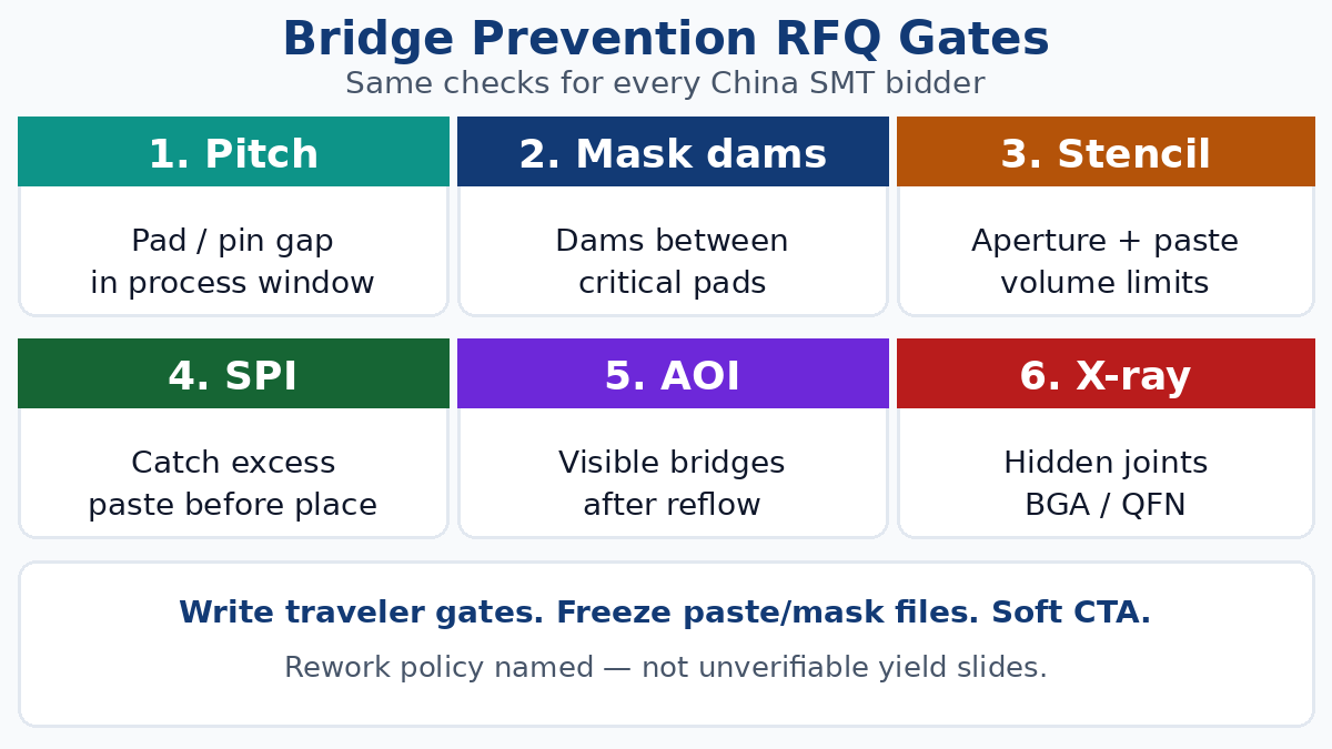
How China SMT lines catch bridges: SPI → AOI → selective X-ray
Export China SMT lines that run denser packages usually stage detection in layers. Buyers should write the stack, not a single magic machine name.
SPI after paste print
Solder paste inspection measures deposit volume and shape before components are placed. Excess paste on fine-pitch pads is cheaper to reprint than to reflow and rework. SPI does not see a finished bridge — it sees the paste condition that often creates one. If your BOM includes 0.4 mm pitch or tighter, ask whether SPI is in the traveler for those lots.
AOI after reflow
Automated optical inspection looks for bridges, insufficient solder, tombstones, polarity, and many other post-reflow defects on visible joints. This page does not rewrite the deep AOI article — it only places AOI as the workhorse bridge catcher on exposed pins and pads. Write AOI coverage expectations (which sides, which packages) on the PO when bridge risk is material.
Selective X-ray for hidden joints
When pads sit under packages (BGA, some QFN/LGA styles), optical cameras cannot see the joint field. Selective X-ray inspection catches shorts and voids in those hidden volumes. Do not demand 100% X-ray on every resistor; do name X-ray where bridges would be invisible to AOI. Broader PCB board testing and inspection menus (including Flying probe for opens/shorts on bare or assembled nets) complement optical and X-ray — they do not replace paste and AOI discipline on SMT bridges.
Honesty: no plant catches every bridge with one tool. SPI reduces paste-driven risk; AOI catches many visible bridges; X-ray covers hidden joints; electrical test and first-power still matter. Write the combination that matches your pitch and package mix.
Rework reality (without inventing yield numbers)
Bridges that escape into rework are usually cleared with wick, braid, or precision iron / hot-air under magnification, then cleaned and re-inspected. That sounds simple until the pin pitch is fine, the mask is damaged, or the same pad bridges twice because paste volume was never fixed upstream.
Buyer-facing truths:
- Rework is not free. Even when the house absorbs scrap, schedule and risk move. Price or policy should be clear before award.
- Root cause beats pad-by-pad heroics. If bridges cluster on the same pins across a lot, fix stencil, paste, or mask — do not scale hand rework as the process plan.
- Re-inspection after rework matters. A cleared bridge can leave residue, mask damage, or a cold joint. AOI or visual criteria after rework should be named.
- Do not invent plant yield %. This guide does not publish XFPCB bridge defect rates, first-pass yield trophies, or IPC award claims. Compare houses on traveler gates, DFM replies, and how they document rework — not on unverifiable percentage slides.
For NPI, prefer a small first-article with SPI + AOI focus on the densest footprints before releasing volume. That is cheaper than discovering a systematic bridge after five hundred boards.
Soft next step
Treat solder bridges as a design-plus-process risk you can gate on the RFQ: pad spacing and mask dams on the CAD side; paste volume, placement force, and stencil hygiene on the line; SPI → AOI → selective X-ray on the traveler; rework policy in plain language. Keep AOI-depth, QA-suite, testing-methods, SMT-benefits, and mask-color siblings in their own lanes — this page only owns bridge prevention and catch for China SMT awards. Soft next step when files are frozen and inspection gates are written: move the award through How to Place an Order with those fields locked — not a brochure callback that reopens paste and AOI after the PO.